- 您现在的位置:买卖IC网 > Datasheet目录345 > NCP1840Q8A6MNTWG (ON Semiconductor)IC LED DRIVER 12CH PROGR 20QFN Datasheet资料下载
参数资料
| 型号: | NCP1840Q8A6MNTWG |
| 厂商: | ON Semiconductor |
| 文件页数: | 14/19页 |
| 文件大小: | 0K |
| 描述: | IC LED DRIVER 12CH PROGR 20QFN |
| 标准包装: | 1 |
| 恒定电流: | 是 |
| 拓扑: | 切换式电容器(充电泵),PWM |
| 输出数: | 8 |
| 内部驱动器: | 是 |
| 类型 - 主要: | 车载,通用 |
| 频率: | 400kHz |
| 电源电压: | 3 V ~ 5.5 V |
| 输出电压: | 4.1V |
| 安装类型: | 表面贴装 |
| 封装/外壳: | 20-VFQFN 裸露焊盘 |
| 供应商设备封装: | 20-QFN(4x4) |
| 包装: | 带卷 (TR) |
| 工作温度: | -40°C ~ 85°C |
�� �
�
�NCP1840�
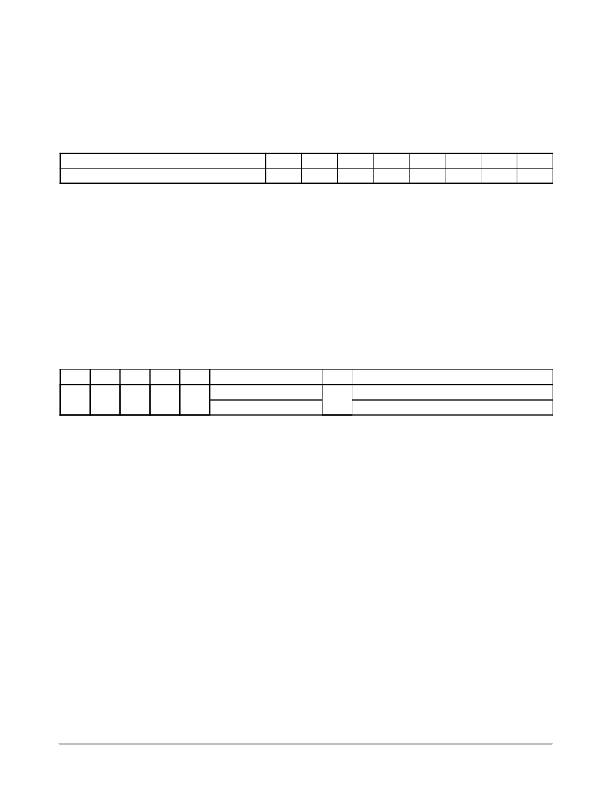
�Output� Control� Register�
�The� Output� Control� Register� on� the� NCP1840� is� used� to�
�set� the� status,� either� ON� or� OFF,� of� all� 8� channels.� As� shown�
�in� the� following� table,� each� bit� in� the� register� corresponds� to�
�one� of� the� 8� LED� channels.� Each� channel� will� be� turned� ON�
�with� a� 1� loaded� into� the� corresponding� bit� and� will� be� turned�
�OUTPUT CONTROL REGISTER DESCRIPTION�
�OFF� with� a� 0� loaded� into� that� bit.� When� an� LED� channel� is�
�turned� ON,� the� current� level� and� PWM� duty� cycle� of� that�
�channel� will� be� dictated� by� the� data� that� is� loaded� into� its�
�Current� Level� Register� and� PWM� Register.� It� is� important� to�
�note� that� any� unused� LED� channel� should� not� be� turned� ON.�
�Register� Bit� (1� =� ON,� 0� =� OFF)�
�Corresponding� LED� Channel�
�D7�
�LED8�
�D6�
�LED7�
�D5�
�LED6�
�D4�
�LED5�
�D3�
�LED4�
�D2�
�LED3�
�D1�
�LED2�
�D0�
�LED1�
�Main� Status� Register�
�The� Main� Status� Register� of� the� NCP1840� is� used� to�
�indicate� the� operating� condition� of� the� part� and� is� read� ?� only.�
�As� shown� in� the� following� table,� bit� D0� indicates� either�
�normal� operation� (0)� or� an� over� temperature� condition� (1).�
�When� the� on� ?� chip� temperature� sensor� detects� an�
�over� ?� temperature� condition,� it� will� turn� off� all� LED� outputs,�
�along� with� the� charge� pump,� and� set� bit� D0� to� a� logic� one.� If�
�the� over� ?� temperature� condition� goes� away,� bit� D0� will�
�automatically� reset� to� a� logic� zero� and� the� part� will� resume�
�normal� operation.� Therefore,� bit� D0� of� this� register� can� be�
�read� and� used� to� help� determine� if� an� over� ?� temperature�
�MAIN� STATUS� REGISTER� DESCRIPTION�
�condition� currently� exists� on� the� part.� Likewise,� bit� D2�
�indicates� either� normal� operation� (0)� or� low� power� mode�
�operation� (1).� When� all� LED� outputs� are� turned� OFF� and�
�there� is� no� I� 2� C� communication� for� 5� ms,� the� part� will� put�
�itself� in� a� low� power� mode� and� set� bit� D2� to� a� logic� one.�
�When� the� Master� wakes� the� device� up� with� I� 2� C�
�communication,� bit� D2� will� be� set� to� a� logic� zero� once� the�
�entire� chip� is� ready� to� run� in� normal� operation.� Therefore,�
�when� the� Master� wakes� up� the� device,� it� can� read� bit� D2� and�
�wait� for� this� bit� to� change� to� 0,� indicating� the� return� to� normal�
�operation.�
�D7�
�0�
�D6�
�0�
�D5�
�0�
�D4�
�0�
�D3�
�0�
�D2�
�0� =� Normal� Operation�
�1� =� Low� Power� Mode�
�D1�
�0�
�D0�
�0� =� Normal� Operation�
�1� =� Over� Temperature�
�Fault� Management�
�The� NCP1840� has� several� fault� management� features�
�intended� to� provide� increased� performance� and� reliability� to�
�both� the� system� and� the� part� itself:�
�?� Each� LED� output� will� detect� if� it� is� shorted� to� the�
�charge� pump� output� and� if� so� will� turn� that� particular�
�channel’s� circuitry� OFF.� This� saves� power� consumption�
�that� would� otherwise� be� lost� and� provides� the� user� with�
�the� ability� to� ensure� that� unused� channels� are� turned�
�OFF� by� tying� them� to� the� charge� pump� output.�
�?� The� charge� pump� output� will� detect� any� over� ?� current�
�events� and� automatically� limit� the� current� to� less� than�
�800� mA.� This� helps� to� prevent� any� damage� to� the� chip�
�and� the� system� due� to� elevated� current� on� this� output.�
�?� The� charge� pump� output� will� detect� a� short� ?� circuit�
�event� (less� than� 0.7� V)� and� limit� the� current� to� the�
�soft� ?� start� limit� of� less� than� 94� mA.� This� helps� to�
�prevent� damage� to� the� chip� and� the� system� that� could�
�potentially� be� seen� with� the� output� being�
�short� ?� circuited� to� ground.�
�?� The� charge� pump� will� reset� itself� to� 1x� mode� if� it�
�reaches� an� overvoltage� level� (5.5� V� to� 6� V).� This� helps�
�?�
�?�
�event� that� the� supply� voltage� increases� while� the� charge�
�pump� is� operating� in� the� 1.33x,� 1.5x,� or� 2x� mode.�
�If� the� external� resistor,� R� BIAS� ,� used� to� set� the� maximum�
�output� current� and� the� internal� reference� current,� is� too�
�small� or� otherwise� short� ?� circuits,� the� NCP1840� will�
�detect� this� over� ?� current� condition� and� turn� off� the�
�reference� current� and� LED� outputs.� This� helps� to�
�prevent� damage� to� the� chip� and� system� due� to� elevated�
�currents� that� would� be� present.�
�The� NCP1840� has� an� on� ?� chip� over� temperature� sensor�
�that� will� detect� any� over� ?� temperature� condition� (130� °� C�
�?� 163� °� C)� and� turn� off� all� LED� outputs� along� with� the�
�charge� pump.� In� an� over� ?� temperature� state,� bit� D0� of�
�the� Main� Status� Register� will� be� set� to� a� logic� one.�
�When� the� over� ?� temperature� condition� goes� away,� the�
�part� will� resume� normal� operation� and� bit� D0� will� be� set�
�to� a� logic� zero.� The� D0� bit� of� the� Main� Status� Register�
�can� be� read� through� the� I� 2� C� interface� and� can� be� used� to�
�provide� feedback� to� the� Master� controller.� This� helps� to�
�protect� the� chip� and� system� in� the� event� that� the�
�temperature� increases� beyond� a� safe� operating�
�condition.�
�to� prevent� damage� to� the� chip� and� the� system� in� the�
�http://onsemi.com�
�14�
�相关PDF资料 |
PDF描述 |
|---|---|
| NCP1910GEVB | BOARD DEMO NCP1910DEMO-B-TLS |
| NCP3418BMNR2G | IC MOSFET DRIVER DUAL 12V 10-DFN |
| NCP3418DR2 | IC MOSFET DRIVER DUAL 12V 8-SOIC |
| NCP3420DR2G | IC MOSFET DRIVER DUAL 12V 8-SOIC |
| NCP3488DR2G | IC MOSFET DRVR DUAL 12V 8-SOIC |
相关代理商/技术参数 |
参数描述 |
|---|---|
| NCP1850FCCT1G | 制造商:ON Semiconductor 功能描述:1.5A SWITCHING BATTERY CH - Tape and Reel 制造商:ON Semiconductor 功能描述:REEL - 1.5A SWITCHING BATTERY CH |
| NCP1851AFCCT1G | 制造商:ON Semiconductor 功能描述:1.8A SWITCHING BATTERY CH - Tape and Reel 制造商:ON Semiconductor 功能描述:REEL / 1.8A SWITCHING BATTERY CH 制造商:ON Semiconductor 功能描述:LINEAR IC |
| NCP1851FCCT1G | 功能描述:电池充电器 RoHS:否 制造商:Power-Sonic 化学性质:Sealed Lead Acid 输出电压:12 V 输出电流:500 mA 端接类型:Screw |
| NCP1852FCCT1G | 制造商:ON Semiconductor 功能描述:BATTERY CHARGER - Tape and Reel |
| NCP18WB333E03RB | 制造商:Murata Manufacturing Co Ltd 功能描述:LEADED NTC THERMISTOR |
发布紧急采购,3分钟左右您将得到回复。