- 您现在的位置:买卖IC网 > PDF目录15269 > NCP300HSN30T1G (ON Semiconductor)IC VOLT DETECT CMOS 3.0V 5TSOP PDF资料下载
参数资料
| 型号: | NCP300HSN30T1G |
| 厂商: | ON Semiconductor |
| 文件页数: | 1/26页 |
| 文件大小: | 0K |
| 描述: | IC VOLT DETECT CMOS 3.0V 5TSOP |
| 标准包装: | 1 |
| 类型: | 简单复位/加电复位 |
| 监视电压数目: | 1 |
| 输出: | 推挽式,图腾柱 |
| 复位: | 高有效 |
| 电压 - 阀值: | 3V |
| 工作温度: | -40°C ~ 125°C |
| 安装类型: | 表面贴装 |
| 封装/外壳: | 6-TSOP(0.059",1.50mm 宽)5 引线 |
| 供应商设备封装: | 5-TSOP |
| 包装: | 剪切带 (CT) |
| 其它名称: | NCP300HSN30T1GOSCT |
�� �
�
�NCP300,� NCP301�
�Voltage� Detector� Series�
�The� NCP300� and� NCP301� series� are� second� generation� ultra� ?� low�
�current� voltage� detectors.� These� devices� are� specifically� designed� for�
�use� as� reset� controllers� in� portable� microprocessor� based� systems�
�where� extended� battery� life� is� paramount.�
�Each� series� features� a� highly� accurate� undervoltage� detector� with�
�hysteresis� which� prevents� erratic� system� reset� operation� as� the�
�http://onsemi.com�
�comparator� threshold� is� crossed.�
�The� NCP300� series� consists� of� complementary� output� devices� that�
�are� available� with� either� an� active� high� or� active� low� reset� output.� The�
�NCP301� series� has� an� open� drain� N� ?� Channel� output� with� either� an�
�active� high� or� active� low� reset� output.�
�The� NCP300� and� NCP301� device� series� are� available� in� the�
�5�
�1�
�THIN� SOT23� ?� 5/�
�TSOP� ?� 5/SC59� ?� 5�
�CASE� 483�
�MARKING� DIAGRAM�
�5�
�xxx� AYW� G�
�G�
�1�
�Thin� TSOP� ?� 5� package� with� standard� undervoltage� thresholds.�
�Additional� thresholds� that� range� from� 0.9� V� to� 4.9� V� in� 100� mV� steps�
�can� be� manufactured.�
�xxx�
�A�
�Y�
�=� Specific� Device� Code�
�=� Assembly� Location�
�=� Year�
�5� N.C.�
�1�
�Features�
�?� Quiescent� Current� of� 0.5� m� A� Typical�
�?� High� Accuracy� Undervoltage� Threshold� of� 2.0%�
�?� Wide� Operating� Voltage� Range� of� 0.8� V� to� 10� V�
�?� Complementary� or� Open� Drain� Reset� Output�
�?� Active� Low� or� Active� High� Reset� Output�
�?� Specified� Over� the� ?� 40� °� C� to� +125� °� C� Temperature� Range�
�(Except� for� Voltage� Options� from� 0.9� to� 1.1� V)�
�?� Pb� ?� Free� Packages� are� Available�
�Typical� Applications�
�?� Microprocessor� Reset� Controller�
�?� Low� Battery� Detection�
�?� Power� Fail� Indicator�
�?� Battery� Backup� Detection�
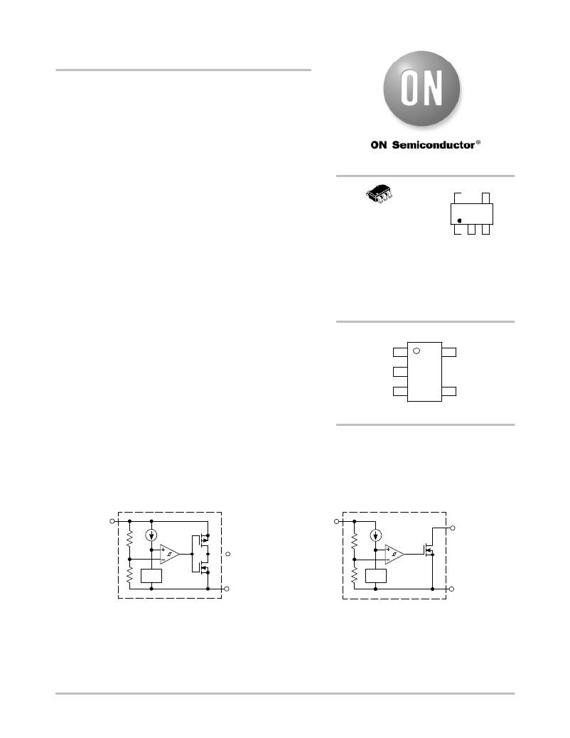
�NCP300xSNxxT1�
�Complementary� Output� Configuration�
�W� =� Work� Week�
�G� =� Pb� ?� Free� Package�
�(Note:Microdot� may� be� in� either� location)�
�PIN� CONNECTIONS�
�Reset�
�Output�
�Input� 2�
�Ground� 3� 4� N.C.�
�(Top� View)�
�ORDERING� INFORMATION�
�See� detailed� ordering� and� shipping� information� in� the� ordering�
�information� section� on� page� 21� of� this� data� sheet.�
�NCP301xSNxxT1�
�Open� Drain� Output� Configuration�
�Input�
�2�
�*�
�1�
�Reset� Output�
�Input�
�2�
�*�
�1�
�Reset� Output�
�V� ref�
�3�
�GND�
�V� ref�
�3�
�GND�
�*� The� representative� block� diagrams� depict� active� low� reset� output� ‘L’� suffix� devices.� The� comparator�
�inputs� are� interchanged� for� the� active� high� output� ‘H’� suffix� devices.�
�This� device� contains� 25� active� transistors.�
�Figure� 1.� Representative� Block� Diagrams�
�?� Semiconductor� Components� Industries,� LLC,� 2009�
�October,� 2009� ?� Rev.� 27�
�1�
�Publication� Order� Number:�
�NCP300/D�
�相关PDF资料 |
PDF描述 |
|---|---|
| VE-251-EW-F3 | CONVERTER MOD DC/DC 12V 100W |
| VE-251-EW-F1 | CONVERTER MOD DC/DC 12V 100W |
| NCP300HSN27T1G | IC VOLT DETECT CMOS 2.7V 5TSOP |
| VI-JTP-EW-F4 | CONVERTER MOD DC/DC 13.8V 100W |
| NCP300HSN18T1G | IC VOLT DETECT CMOS 1.8V 5TSOP |
相关代理商/技术参数 |
参数描述 |
|---|---|
| NCP300HSN31T1 | 制造商:ONSEMI 制造商全称:ON Semiconductor 功能描述:Voltage Detector Series |
| NCP300HSN32T1 | 制造商:ONSEMI 制造商全称:ON Semiconductor 功能描述:Voltage Detector Series |
| NCP300HSN33T1 | 制造商:ONSEMI 制造商全称:ON Semiconductor 功能描述:Voltage Detector Series |
| NCP300HSN34T1 | 制造商:ONSEMI 制造商全称:ON Semiconductor 功能描述:Voltage Detector Series |
| NCP300HSN35T1 | 制造商:ONSEMI 制造商全称:ON Semiconductor 功能描述:Voltage Detector Series |
发布紧急采购,3分钟左右您将得到回复。