- 您现在的位置:买卖IC网 > PDF目录15265 > NCP300LSN47T1G (ON Semiconductor)IC VOLT DETECT CMOS 4.7V 5TSOP PDF资料下载
参数资料
| 型号: | NCP300LSN47T1G |
| 厂商: | ON Semiconductor |
| 文件页数: | 16/26页 |
| 文件大小: | 0K |
| 描述: | IC VOLT DETECT CMOS 4.7V 5TSOP |
| 标准包装: | 1 |
| 类型: | 简单复位/加电复位 |
| 监视电压数目: | 1 |
| 输出: | 推挽式,图腾柱 |
| 复位: | 低有效 |
| 电压 - 阀值: | 4.7V |
| 工作温度: | -40°C ~ 125°C |
| 安装类型: | 表面贴装 |
| 封装/外壳: | 6-TSOP(0.059",1.50mm 宽)5 引线 |
| 供应商设备封装: | 5-TSOP |
| 包装: | 剪切带 (CT) |
| 其它名称: | NCP300LSN47T1GOSCT |
�� �
�
�NCP300,� NCP301�
�So,� V� DET+_max� can� be� easily� figured� out� just� using� a� single�
�variable� V� DET� ?� _typ� .�
�For� example,� for� NCP300LSN18T1G� V� DET� ?� _typ� =� 1.8� V;�
�then�
�V� DET+_max� +� 1.8� 1.09� +� 1.962� V� (eq.� 8)�
�The� NCP30X� detection� voltage� option� must� be� chosen� such�
�that:�
�V� CC_min� t� V� DET+_max� t� V� in_min� (eq.� 9)�
�PROPAGATION� DELAY� VARIATION�
�On� the� other� hand� (see� above� paragraph),� a� minimum�
�overdrive� value� from� V� threshold� to� V� CC� must� be� respected.�
�That� means� V� in� (minimum� value� of� V� CC� )� must� be� higher�
�enough� than� V� DET+� (V� DET� ?� +� hysteresis)� at� the� risk� of�
�significantly� increasing� propagation� delay.� (Figure� 25)� This�
�propagation� delay� is� temperature� sensitive.�
�To� avoid� acceptable� time� response,� a� minimum� 100� mV�
�difference� between� V� in� and� V� DET+� must� be� selected.�
�The� significance� of� V� CC_min� <� V� DET+_max� is� that� it� makes�
�sure� the� the� reset� from� NCP30X� remains� asserted� (in� RESET�
�hold� state)� till� after� the� power� supply� exceeds� the� V� CC_min�
�requirement;� this� prevents� incorrect� device� (uP)� initiation.�
�Having� V� DET+_max� <� V� in_min� makes� sure� that� the�
�NCP30X� is� able� to� start� up� when� V� in� is� at� the� V� in_min� .�
�The� theoretical� ideal� V� DET� ?� _typ� voltage� option� to� be�
�selected� by� the� user,� V� DET� ?� _typ_ideal� ,� can� be� given� by� the�
�following� formula:�
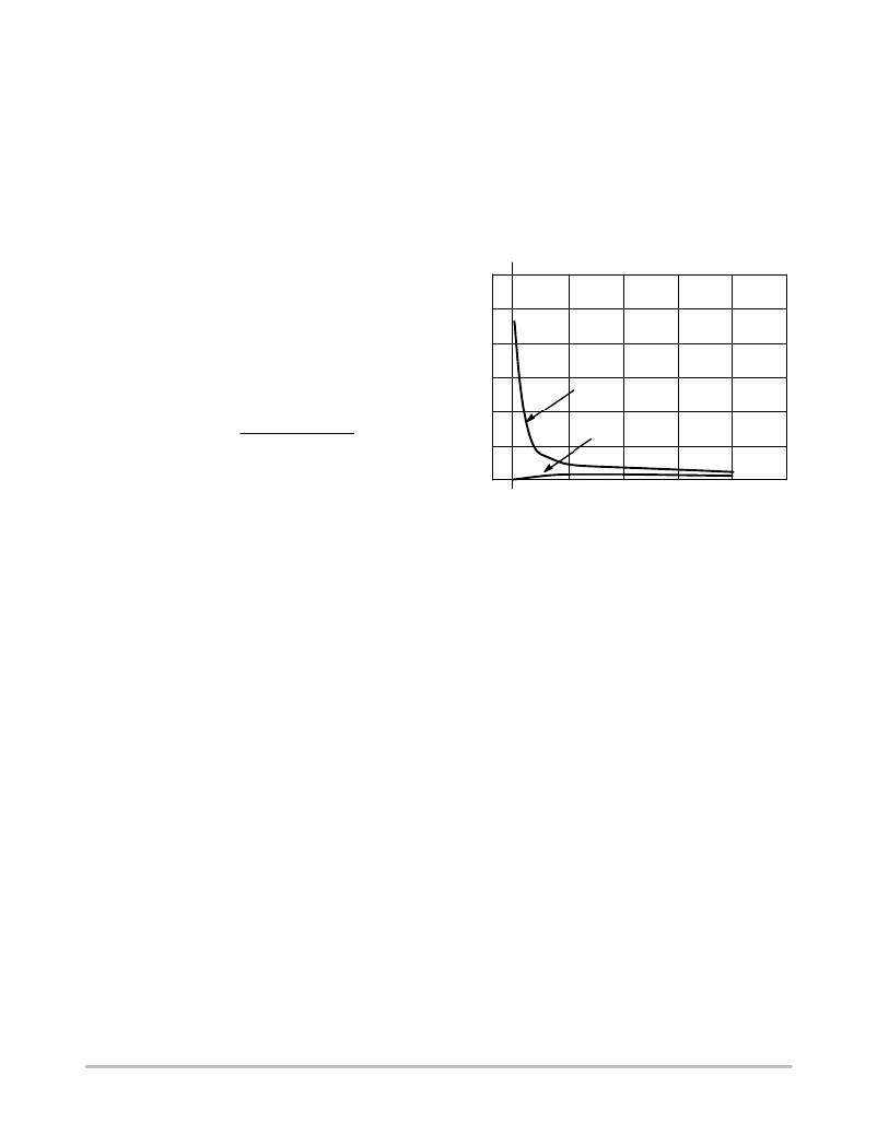
�600�
�500�
�400�
�300�
�V� DET+�
�t� pHL�
�V� DET� ?� _typ_ideal� +�
�V� in_min� )� V� CC_min�
�(2� 1.09)�
�(eq.� 10)�
�200�
�100�
�t� pLH�
�3.168�
�The� following� example� shows� how� to� select� the� device�
�voltage� option� in� a� real� world� application.�
�1.� Power� supply� output� specification:� 3.3� V� $� 3%�
�2.� Microprocessor� core� voltage� specification:� 3.3� V�
�$� 5%�
�So,� we� have:�
�V� in_min� +� 3.3� V� *� 3%� +� 3.201� V� (eq.� 11)�
�V� CC_min� +� 3.3� V� *� 5%� +� 3.135� V�
�(eq.� 12)�
�0�
�3.0� 3.5� 4.0� 4.5� 5.0�
�V� in� ,� PULSE� HIGH� INPUT� VOLTAGE� (V)�
�Figure� 25.� t� pLH� and� t� pHL� vs.� Input� Voltage�
�for� the� NCP301SNT1�
�5.5�
�Then� the� ideal� voltage� option� =� (3.201� +� 3.135)� /� (2� *� 1.09)�
�=� 2.9064� V�
�Therefore,� a� device� voltage� option� of� 2.9� V� will� be� the� right�
�choice.�
�http://onsemi.com�
�16�
�相关PDF资料 |
PDF描述 |
|---|---|
| H2AXT-10112-B4-ND | JUMPER-H1502TR/A2015B/X 12" |
| RSM12DSEH-S13 | CONN EDGECARD 24POS .156 EXTEND |
| VE-2TF-EY-B1 | CONVERTER MOD DC/DC 72V 50W |
| H2AXT-10112-A4-ND | JUMPER-H1502TR/A2015A/X 12" |
| NCP300LSN46T1G | IC VOLT DETECT CMOS 4.6V 5TSOP |
相关代理商/技术参数 |
参数描述 |
|---|---|
| NCP300LSN48T1 | 制造商:Rochester Electronics LLC 功能描述:- Tape and Reel 制造商:ON Semiconductor 功能描述: |
| NCP300LSN49T1 | 制造商:Rochester Electronics LLC 功能描述:- Bulk 制造商:ON Semiconductor 功能描述: |
| NCP301 | 制造商:ONSEMI 制造商全称:ON Semiconductor 功能描述:Voltage Detector Series |
| NCP3011 | 制造商:ONSEMI 制造商全称:ON Semiconductor 功能描述:Synchronous PWM Controller |
| NCP3011DTBR2G | 功能描述:电压模式 PWM 控制器 Single Output Buck 0.8V to 40V 70uA RoHS:否 制造商:Texas Instruments 输出端数量:1 拓扑结构:Buck 输出电压:34 V 输出电流: 开关频率: 工作电源电压:4.5 V to 5.5 V 电源电流:600 uA 最大工作温度:+ 125 C 最小工作温度:- 40 C 封装 / 箱体:WSON-8 封装:Reel |
发布紧急采购,3分钟左右您将得到回复。