- 您现在的位置:买卖IC网 > PDF目录17195 > NCP3065SOBSTGEVB (ON Semiconductor)EVAL BOARD FOR NCP3065SOBSTG PDF资料下载
参数资料
| 型号: | NCP3065SOBSTGEVB |
| 厂商: | ON Semiconductor |
| 文件页数: | 7/18页 |
| 文件大小: | 0K |
| 描述: | EVAL BOARD FOR NCP3065SOBSTG |
| 设计资源: | NCP3065 Boost Eval Board BOM NCP3065SOBSTGEVB Gerber Files NCP3065 Boost Eval Board Schematic |
| 标准包装: | 1 |
| 电流 - 输出 / 通道: | 350mA |
| 输出及类型: | 1,非隔离 |
| 输出电压: | 20V |
| 输入电压: | 12V |
| 已供物品: | 板 |
| 已用 IC / 零件: | NCP3065 |
| 其它名称: | NCP3065SOBSTGEVBOS |
�� �
�
�NCP3065,� NCV3065�
�INTRODUCTION�
�The� NCP3065� is� a� monolithic� power� switching� regulator�
�optimized� for� LED� Driver� applications.� Its� flexible�
�architecture� enables� the� system� designer� to� directly�
�implement� a� step� ?� up� or� step� ?� down� topology� with� a�
�minimum� number� of� external� components� for� driving� LEDs.�
�A� representative� block� diagram� is� shown� in� Figure� 4.�
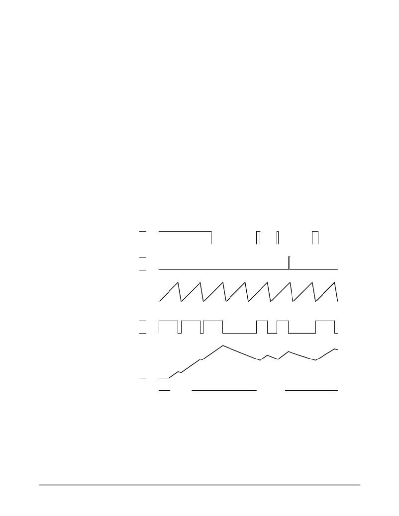
�OPERATING� DESCRIPTION�
�The� NCP3065� operates� as� a� fixed� oscillator� frequency�
�output� voltage� ripple� gated� regulator.� In� general,� this� mode�
�of� operation� is� somewhat� analogous� to� a� capacitor� charge�
�pump� and� does� not� require� dominant� pole� loop�
�compensation� for� converter� stability.� The� typical� operating�
�waveforms� are� shown� in� Figure� 14.� The� output� voltage�
�waveform� shown� is� for� a� step� ?� down� converter� with� the�
�ripple� and� phasing� exaggerated� for� clarity.� During� initial�
�converter� startup,� the� feedback� comparator� senses� that� the�
�output� voltage� level� is� below� nominal.� This� causes� the�
�output� switch� to� turn� on� and� off� at� a� frequency� and� duty� cycle�
�controlled� by� the� oscillator,� thus� pumping� up� the� output� filter�
�capacitor.� When� the� feedback� voltage� level� reaches� nominal�
�comparator� value,� the� output� switch� cycle� is� inhibited.� When�
�the� load� current� causes� the� output� voltage� to� fall� below� the�
�nominal� value� feedback� comparator� enables� switching�
�immediately.� Under� these� conditions,� the� output� switch�
�conduction� can� be� enabled� for� a� partial� oscillator� cycle,� a�
�partial� cycle� plus� a� complete� cycle,� multiple� cycles,� or� a�
�partial� cycle� plus� multiple� cycles.�
�Oscillator�
�The� oscillator� frequency� and� off� ?� time� of� the� output� switch�
�are� programmed� by� the� value� of� the� timing� capacitor� C� T� .�
�Capacitor� C� T� is� charged� and� discharged� by� a� 1� to� 6� ratio�
�internal� current� source� and� sink,� generating� a� positive� going�
�sawtooth� waveform� at� Pin� 3.� This� ratio� sets� the� maximum�
�t� ON� /(t� ON� +t� OFF� )� of� the� switching� converter� as� 6/(6+1)� or�
�85.7%� (typical).� The� oscillator� peak� and� valley� voltage�
�difference� is� 500� mV� typically.� To� calculate� the� C� T� capacitor�
�value� for� required� oscillator� frequency,� use� the� equations�
�found� in� Figure� 22.� An� online� NCP3065� design� tool� can� be�
�found� at� www.onsemi.com,� which� adds� in� selecting�
�component� values.�
�Feedback� Comparator� Output�
�I� PK� Comparator� Output�
�1�
�0�
�1�
�0�
�Timing� Capacitor,� C� T�
�Output� Switch�
�On�
�Off�
�Nominal� Output� Voltage� Level�
�Output� Voltage�
�Startup�
�Figure� 14.� Typical� Operating� Waveforms�
�http://onsemi.com�
�7�
�Operation�
�相关PDF资料 |
PDF描述 |
|---|---|
| RNM-3.305S/H | CONV DC/DC 1W 3.3VIN 05VOUT |
| TC1410NEOA713 | IC MOSFET DVR .5A HS 8SOIC |
| EEM06DTAT-S189 | CONN EDGECARD 12POS R/A .156 SLD |
| GEM18DRXN | CONN EDGECARD 36POS DIP .156 SLD |
| TC1410EOA713 | IC MOSFET DVR .5A HS INV 8SOIC |
相关代理商/技术参数 |
参数描述 |
|---|---|
| NCP3066DFSEPGEVB | 功能描述:电源管理IC开发工具 NCP3066 DFN SEPIC DB RoHS:否 制造商:Maxim Integrated 产品:Evaluation Kits 类型:Battery Management 工具用于评估:MAX17710GB 输入电压: 输出电压:1.8 V |
| NCP3066DR2G | 功能描述:直流/直流开关调节器 1.5A SW REG FOR LED W/ENABLE RoHS:否 制造商:International Rectifier 最大输入电压:21 V 开关频率:1.5 MHz 输出电压:0.5 V to 0.86 V 输出电流:4 A 输出端数量: 最大工作温度: 安装风格:SMD/SMT 封装 / 箱体:PQFN 4 x 5 |
| NCP3066MNTXG | 功能描述:直流/直流开关调节器 1.5A SW REG FOR LED W/ENABLE RoHS:否 制造商:International Rectifier 最大输入电压:21 V 开关频率:1.5 MHz 输出电压:0.5 V to 0.86 V 输出电流:4 A 输出端数量: 最大工作温度: 安装风格:SMD/SMT 封装 / 箱体:PQFN 4 x 5 |
| NCP3066PG | 功能描述:直流/直流开关调节器 1.5A SW REG FOR LED W/ENABLE RoHS:否 制造商:International Rectifier 最大输入电压:21 V 开关频率:1.5 MHz 输出电压:0.5 V to 0.86 V 输出电流:4 A 输出端数量: 最大工作温度: 安装风格:SMD/SMT 封装 / 箱体:PQFN 4 x 5 |
| NCP3066S3BCKGEVB | 功能描述:电源管理IC开发工具 NCP3066 3A SOIC BUCK DB RoHS:否 制造商:Maxim Integrated 产品:Evaluation Kits 类型:Battery Management 工具用于评估:MAX17710GB 输入电压: 输出电压:1.8 V |
发布紧急采购,3分钟左右您将得到回复。