参数资料
| 型号: | NCP348AEMTTXG |
| 厂商: | ON Semiconductor |
| 文件页数: | 10/13页 |
| 文件大小: | 0K |
| 描述: | IC MOSFET DRIVER DUAL 12V 10WDFN |
| 产品变化通告: | Product Obsolescence 13/Apr/2009 |
| 标准包装: | 10,000 |
| 电压 - 工作: | 1.2 ~ 28V |
| 电压 - 箝位: | 6.4V |
| 技术: | 混合技术 |
| 电路数: | 3 |
| 应用: | 通用 |
| 封装/外壳: | 10-WFDFN 裸露焊盘 |
| 供应商设备封装: | 10-WDFN(2.5x2) |
| 包装: | 带卷 (TR) |
�� �
�
�NCP348,� NCP348AE�
�Undervoltage� Lockout� (UVLO)�
�To� ensure� proper� operation� under� any� conditions,� the�
�device� has� a� built� ?� in� undervoltage� lockout� (UVLO)� circuit.�
�During� V� in� positive� going� slope,� the� output� remains�
�disconnected� from� input� until� V� in� voltage� is� below� 3.25� V�
�(NCP348MTT� version),� plus� hysteresis,� nominal.� The�
�FLAG� output� is� tied� to� low� as� long� as� V� in� does� not� reach�
�UVLO� threshold.� This� circuit� has� a� 50� mV� hysteresis� to�
�provide� noise� immunity� to� transient� condition.� Additional�
�UVLO� thresholds� ranging� from� UVLO� can� be�
�manufactured.� (See� Selection� Guide� on� page� 12)� Contact�
�your� ON� Semiconductor� representative� for� availability.�
�Overvoltage� Lockout� (OVLO)�
�To� protect� connected� systems� on� V� out� pin� from�
�overvoltage,� the� device� has� a� built� ?� in� overvoltage� lockout�
�(OVLO)� circuit.� During� overvoltage� condition,� the� output�
�remains� disabled� as� long� as� the� input� voltage� exceeds� 6.4� V�
�typical� (NCP348MTT� version).� Additional� OVLO�
�thresholds� ranging� from� OVLO� can� be� manufactured.� (See�
�Selection� Guide� on� page� 12)� Contact� your� ON�
�Semiconductor� representative� for� availability.�
�FLAG� output� is� tied� to� low� until� V� in� is� higher� than� OVLO.�
�This� circuit� has� a� 100� mV� hysteresis� to� provide� noise�
�immunity� to� transient� conditions� .�
�FLAG� Output�
�The� NCP348� provides� a� FLAG� output,� which� alerts�
�external� systems� that� a� fault� has� occurred.�
�This� pin� is� tied� to� low� as� soon� the� OVLO� threshold� is�
�exceeded� or� when� the� V� in� level� is� below� the� UVLO�
�threshold.� When� V� in� level� recovers� normal� condition,�
�FLAG� is� held� high,� keeping� in� mind� that� an� additional�
�50 ms� delay� has� been� added� between� available� output� and�
�FLAG� =� high.� The� pin� is� an� open� drain� output,� thus� a� pull�
�up� resistor� (typically� 1� M� W� ,� minimum� 10� k� W� )� must� be�
�added� to� V� bat� .� Minimum� V� bat� supply� must� be� 2.5� V.� The�
�FLAG� level� will� always� reflects� V� in� status,� even� if� the�
�device� is� turned� off� (EN� =� 1).�
�EN� Input�
�To� enable� normal� operation,� the� EN� pin� shall� be� forced�
�to� low� or� connected� to� ground.� A� high� level� on� the� pin,�
�disconnects� OUT� pin� from� IN� pin.� EN� does� not� overdrive�
�an� OVLO� or� UVLO� fault.�
�Internal� NMOS� FET�
�The� NCP348� includes� an� internal� Low� R� DS(on)� NMOS�
�FET� to� protect� the� systems,� connected� on� OUT� pin,� from�
�positive� overvoltage.� Regarding� electrical� characteristics,�
�the� R� DS(on)� ,� during� normal� operation,� will� create� low� losses�
�on� V� out� pin.�
�As� example:� R� load� =� 8.0� W� ,� V� in� =� 5.0� V�
�Typical� R� DS(on)� =� 65� m� W,� I� out� =� 618� mA�
�V� out� =� 8� x� 0.618� =� 4.95� V�
�NMOS� losses� =� R� DS(on)� x� Iout� 2� =� 0.065� x� 0.618� 2� =� 25� mW�
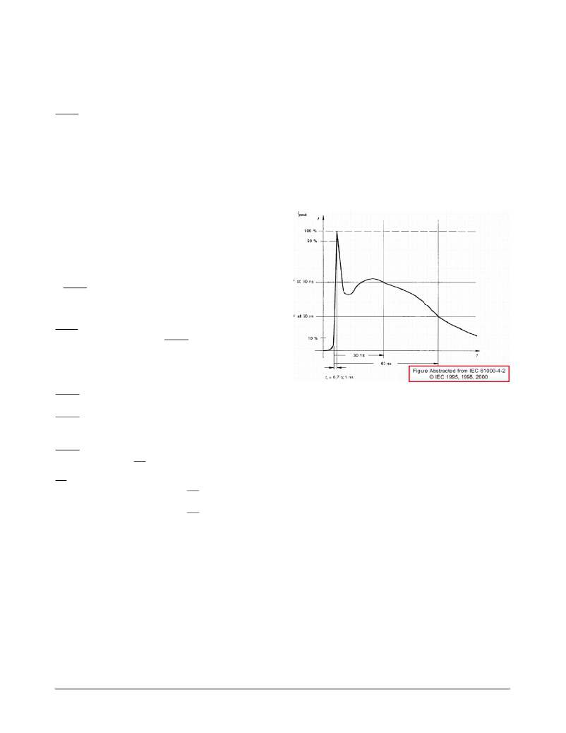
�ESD� Tests�
�The� NCP348� input� pin� fully� supports� the� IEC61000� ?� 4� ?� 2.�
�1.0� m� F� (minimum)� must� be� connected� between� V� in� and�
�GND,� close� to� the� device.�
�That� means,� in� Air� condition,� V� in� has� a� "� 15� kV� ESD�
�protected� input.� In� Contact� condition,� V� in� has� "� 8.0� kV�
�ESD� protected� input.�
�Please� refer� to� Figure� 19� to� see� the� IEC� 61000� ?� 4� ?� 2�
�electrostatic� discharge� waveform.�
�Figure� 19.� Electrostatic� Discharge� Waveform�
�PCB� Recommendations�
�The� NCP348� integrates� a� 2� amperes� rated� NMOS� FET,�
�and� the� PCB� rules� must� be� respected� to� properly� evacuate�
�the� heat� out� of� the� silicon.� The� PAD1� is� internally� isolated�
�from� the� active� silicon� and� should� preferably� be� connected�
�to� ground.� The� PAD2� of� the� NCP348� package� is� connected�
�to� the� internal� NMOS� drain� and� can� be� used� to� increase� the�
�heat� transfer� if� necessary� from� an� applications� standpoint.�
�Depending� upon� the� power� dissipated� in� the� application,�
�one� can� either� use� the� PCB� tracks� connected� to� Pins� 4� and�
�5� to� evacuate� heat,� or� make� profit� of� the� PAD2� area� to� add�
�extra� copper� surface� to� reduce� the� junction� temperature�
�(See� Figure� 20).� Of� course,� in� any� case,� this� pad� shall� be� not�
�connected� to� any� other� potential.� Figure� 20� shows� copper�
�area� according� to� R� q� JA� and� allows� the� design� of� the� heat�
�transfer� plane� connected� to� PAD2.�
�http://onsemi.com�
�10�
�相关PDF资料 |
PDF描述 |
|---|---|
| AD8000YRDZ-REEL | IC OPAMP CF LN 100MA 8SOIC |
| MMS-140-02-L-SV | CONN RCPT 2MM 40POS SGL VERT SMD |
| TA35-CBTBF100C0 | CIRC BREAKER/BLACK ROCKER 2P 10A |
| SQT-150-01-L-S | CONN RCPT 2MM 50POS SGL VERT PCB |
| NUS3045MNT1 | IC OVP W/30V P-CH MOSFET DFN8 |
相关代理商/技术参数 |
参数描述 |
|---|---|
| NCP348AEMUTBG | 功能描述:监控电路 POSTIVE OVP PRTCTION RoHS:否 制造商:STMicroelectronics 监测电压数: 监测电压: 欠电压阈值: 过电压阈值: 输出类型:Active Low, Open Drain 人工复位:Resettable 监视器:No Watchdog 电池备用开关:No Backup 上电复位延迟(典型值):10 s 电源电压-最大:5.5 V 最大工作温度:+ 85 C 安装风格:SMD/SMT 封装 / 箱体:UDFN-6 封装:Reel |
| NCP348GEVB | 功能描述:电源管理IC开发工具 EVALUATION BRD DEV RoHS:否 制造商:Maxim Integrated 产品:Evaluation Kits 类型:Battery Management 工具用于评估:MAX17710GB 输入电压: 输出电压:1.8 V |
| NCP348GEVB | 制造商:ON Semiconductor 功能描述:Positive Overvoltage Protection Controll |
| NCP348MTTBG | 功能描述:监控电路 OVER VLTG PROTECTION RoHS:否 制造商:STMicroelectronics 监测电压数: 监测电压: 欠电压阈值: 过电压阈值: 输出类型:Active Low, Open Drain 人工复位:Resettable 监视器:No Watchdog 电池备用开关:No Backup 上电复位延迟(典型值):10 s 电源电压-最大:5.5 V 最大工作温度:+ 85 C 安装风格:SMD/SMT 封装 / 箱体:UDFN-6 封装:Reel |
| NCP348MTTXG | 功能描述:监控电路 POS OVR PROTCT CNTRL RoHS:否 制造商:STMicroelectronics 监测电压数: 监测电压: 欠电压阈值: 过电压阈值: 输出类型:Active Low, Open Drain 人工复位:Resettable 监视器:No Watchdog 电池备用开关:No Backup 上电复位延迟(典型值):10 s 电源电压-最大:5.5 V 最大工作温度:+ 85 C 安装风格:SMD/SMT 封装 / 箱体:UDFN-6 封装:Reel |
发布紧急采购,3分钟左右您将得到回复。