- 您现在的位置:买卖IC网 > PDF目录19985 > NCP4632BDT08T5G (ON Semiconductor)IC REG LDO 0.8V 3A DPAK-5 PDF资料下载
参数资料
| 型号: | NCP4632BDT08T5G |
| 厂商: | ON Semiconductor |
| 文件页数: | 12/14页 |
| 文件大小: | 0K |
| 描述: | IC REG LDO 0.8V 3A DPAK-5 |
| 标准包装: | 3,000 |
| 稳压器拓扑结构: | 正,固定式 |
| 输出电压: | 0.8V |
| 输入电压: | 1.6 V ~ 5.25 V |
| 电压 - 压降(标准): | 0.91V @ 3A |
| 稳压器数量: | 1 |
| 电流 - 输出: | 3A(最小) |
| 工作温度: | -40°C ~ 85°C |
| 安装类型: | 表面贴装 |
| 封装/外壳: | TO-252-6,DPak(5 引线 + 接片) |
| 供应商设备封装: | D-Pak 5-引线 |
| 包装: | 带卷 (TR) |
| 其它名称: | NCP4632BDT08T5G-ND NCP4632BDT08T5GOSTR |
�� �
�
�NCP4632�
�APPLICATION� INFORMATION�
�A� typical� application� circuit� for� NCP4632� series� is� shown�
�in� Figure� 38.�
�V� OUT� +� 0.8�
�1� )�
�R1�
�R2�
�)� R1�
�I� ADJ�
�(eq.� 1)�
�VIN�
�NCP4632� (Fixed)�
�VOUT�
�The� current� consumption� I� ADJ� flowing� into� the� ADJ� pin�
�can� be� described� by� Equation� 2.�
�VIN�
�VOUT�
�R1�
�I� ADJ� +� V� SET�
�R1�
�RADJ�
�(eq.� 2)�
�GND�
�C1�
�10� m�
�CE�
�SENSE�
�C2�
�10� m�
�By� choosing� R1� <<� R� ADJ� (R� ADJ� is� typically� around�
�1.6� M� W� ),� this� value� becomes� very� small� in� which� case� we�
�can� omit� the� term� R1� x� I� ADJ� in� Equation� 1.� The� simplified�
�equation� for� the� output� voltage� calculation� is� shown� in�
�Equation� 3.�
�V� OUT� +� 0.8�
�1� )�
�R1�
�VIN�
�NCP4632� (Adj)�
�VIN� VOUT�
�R1�
�VOUT�
�(eq.� 3)�
�R2�
�The� resistor� divider� should� be� kept� to� values� below�
�500� k� W� to� ensure� stability.�
�C1�
�10� m�
�CE�
�GND�
�VADJ�
�R2�
�C2�
�10� m�
�Figure� 38.� Typical� Application� Schematic�
�Input� Decoupling� Capacitor� (C1)�
�A� 10� m� F� ceramic� input� decoupling� capacitor� should� be�
�connected� as� close� as� possible� to� the� input� and� ground� pin� of�
�oncapc7EG�
�V� SET�
�V� OUT�
�the� NCP4632.� Higher� values� and� lower� ESR� improves� line�
�transient� response.�
�Output� Decoupling� Capacitor� (C2)�
�A� 10� m� F� ceramic� output� decoupling� capacitor� is� sufficient�
�to� achieve� stable� operation� of� the� IC.� If� a� tantalum� capacitor�
�is� used,� and� its� ESR� is� high,� loop� oscillation� may� result.�
�Using� multiple� ceramic� capacitors� in� parallel� should� be�
�avoided� if� possible� as� this� can� lead� to� unstable� operation.� The�
�Output� capacitor� should� be� connected� as� close� as� possible� to�
�the� output� and� ground� pin.� Larger� capacitance� values� and�
�lower� ESR� improves� dynamic� parameters.�
�Enable� Operation�
�The� Enable� pin� (CE)� may� be� used� for� turning� the� regulator�
�on� and� off.� The� regulator� is� switched� on� when� the� CE� pin�
�voltage� is� above� logic� high� level.� The� Enable� pin� has� an�
�internal� pull� down� current� source� with� a� 300� nA� current�
�capability.� If� the� enable� function� is� not� needed,� connect� CE�
�pin� to� VIN� pin.�
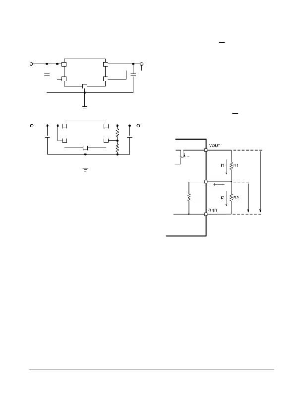
�Output� Voltage� Setting�
�For� the� Adjustable� version� of� the� NCP4632,� the� output�
�voltage� can� be� adjusted� by� using� an� external� resister� divider.�
�Figure� 39.� Output� Voltage� Setting�
�Output� Discharger�
�The� D� version� includes� a� transistor� between� VOUT� and�
�GND� that� is� used� for� faster� discharging� of� the� output�
�capacitor.� This� function� is� activated� when� the� IC� goes� into�
�disable� mode.�
�Thermal�
�As� power� across� the� IC� increases,� it� might� become�
�necessary� to� provide� some� thermal� relief.� The� maximum�
�power� dissipation� supported� by� the� device� is� dependent�
�upon� board� design� and� layout.� Mounting� pad� configuration�
�on� the� PCB,� the� board� material,� and� also� the� ambient�
�temperature� affect� the� rate� of� temperature� rise� for� the� part.�
�That� is� to� say,� when� the� device� has� good� thermal�
�conductivity� through� the� PCB,� the� junction� temperature� will�
�be� relatively� low� with� high� power� dissipation� applications.�
�The� output� voltage� can� be� calculated� using� Equation� 1.�
�http://onsemi.com�
�12�
�相关PDF资料 |
PDF描述 |
|---|---|
| ABC40DRTI | CONN EDGECARD 80POS .100 DIP SLD |
| TAP106K006SCS | CAP TANT 10UF 6.3V 10% RADIAL |
| RGZ-0915D/HP | CONV DC/DC 2W 09VIN +/-15VOUT |
| RGZ-0912D/HP | CONV DC/DC 2W 09VIN +/-12VOUT |
| ABC25DRAI | CONN EDGECARD 50POS .100 R/A DIP |
相关代理商/技术参数 |
参数描述 |
|---|---|
| NCP4632DDT08EVB | 制造商:ON Semiconductor 功能描述:PO - LDO & VREGS - Bulk |
| NCP4632DDT08T5G | 功能描述:低压差稳压器 - LDO 3A LOW INPUT VOLTAGE LDO RoHS:否 制造商:Texas Instruments 最大输入电压:36 V 输出电压:1.4 V to 20.5 V 回动电压(最大值):307 mV 输出电流:1 A 负载调节:0.3 % 输出端数量: 输出类型:Fixed 最大工作温度:+ 125 C 安装风格:SMD/SMT 封装 / 箱体:VQFN-20 |
| NCP4632DDT15EVB | 制造商:ON Semiconductor 功能描述:PO - LDO & VREGS - Bulk |
| NCP4632DDT15T5G | 功能描述:低压差稳压器 - LDO 3A LOW INPUT VOLTAGE LDO RoHS:否 制造商:Texas Instruments 最大输入电压:36 V 输出电压:1.4 V to 20.5 V 回动电压(最大值):307 mV 输出电流:1 A 负载调节:0.3 % 输出端数量: 输出类型:Fixed 最大工作温度:+ 125 C 安装风格:SMD/SMT 封装 / 箱体:VQFN-20 |
| NCP4632DDT28EVB | 制造商:ON Semiconductor 功能描述:PO - LDO & VREGS - Bulk |
发布紧急采购,3分钟左右您将得到回复。