参数资料
| 型号: | NCP4671DMX12TCG |
| 厂商: | ON Semiconductor |
| 文件页数: | 19/23页 |
| 文件大小: | 0K |
| 描述: | IC REG LDO 1.2V .4A 6XDFN |
| 标准包装: | 1 |
| 稳压器拓扑结构: | 正,固定式 |
| 输出电压: | 1.2V |
| 输入电压: | 2.4 V ~ 5.25 V |
| 电压 - 压降(标准): | 0.28V @ 400mA |
| 稳压器数量: | 1 |
| 电流 - 输出: | 400mA(最小) |
| 工作温度: | -40°C ~ 85°C |
| 安装类型: | 表面贴装 |
| 封装/外壳: | 6-XFDFN |
| 供应商设备封装: | 6-XDFN(1.2x1.2) |
| 包装: | 标准包装 |
| 其它名称: | NCP4671DMX12TCGOSDKR |
�� �
�
�NCP4671�
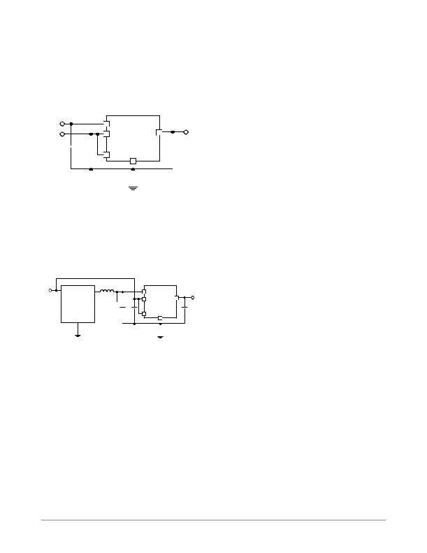
�APPLICATION� INFORMATION�
�A� typical� application� circuit� for� the� NCP4671� series� is�
�shown� in� Figure� 63.� The� NCP4671� has� two� independent�
�inputs,� VBIAS� pin� is� used� for� powering� control� part� of� the�
�LDO� and� its� value� is� equal� or� higher� than� value� of� second�
�input� pin� VIN� where� voltage� that� has� to� be� regulated� is�
�connected.�
�NCP4671x�
�and� ground� pin� of� the� NCP4671.� Higher� values� and� lower�
�ESR� of� capacitor� C1� improves� line� transient� response.�
�Output� Decoupling� Capacitor� (C3)�
�A� 2.2� m� F� or� larger� ceramic� output� decoupling� capacitor� is�
�sufficient� to� achieve� stable� operation� of� the� IC.� If� a� tantalum�
�capacitor� is� used,� and� its� ESR� is� high,� loop� oscillation� may�
�result.� The� capacitors� should� be� connected� as� close� as�
�VIN�
�VBIAS�
�VIN�
�VBIAS�
�VOUT�
�VOUT�
�possible� to� the� output� and� ground� pins.� Larger� values� and�
�lower� ESR� improves� dynamic� parameters.�
�C1�
�1� m�
�C2�
�1� m�
�CE�
�GND�
�C3�
�2� m� 2�
�Enable� Operation�
�The� enable� pin� CE� may� be� used� for� turning� the� regulator�
�on� and� off.� The� regulator� is� switched� on� when� CE� pin� voltage�
�is� above� logic� high� level.� The� enable� pin� has� an� internal� pull�
�down� current� source.� If� the� enable� function� is� not� needed�
�connect� CE� pin� to� VBIAS.�
�Figure� 63.� Typical� Application� Schematic�
�Dual� rail� architecture� is� appropriate� when� the� regulator� is�
�connected� for� example� behind� a� buck� DC/DC� converter.�
�Bias� voltage� can� be� taken� from� input� of� the� buck� DC/DC�
�converter� and� as� input� voltage� is� used� output� of� the� buck�
�DC/DC� converter� as� it� is� shown� in� Figure� 64.� Condition� that�
�bias� voltage� must� be� higher� than� input� voltage� can� be� in� this�
�schematic� easy� fulfilled.�
�Output� Discharger�
�The� D� version� includes� a� transistor� between� VOUT� and�
�GND� that� is� used� for� faster� discharging� of� the� output�
�capacitor.� This� function� is� activated� when� the� IC� goes� into�
�disable� mode.�
�Thermal�
�As� power� across� the� IC� increases,� it� might� become�
�necessary� to� provide� some� thermal� relief.� The� maximum�
�power� dissipation� supported� by� the� device� is� dependent�
�VIN�
�DC/DC�
�converter�
�C1�
�1� m�
�C2�
�1� m�
�NCP4671x�
�VIN�
�VBIAS� VOUT�
�CE� GND�
�VOUT�
�C3�
�2� m� 2�
�upon� board� design� and� layout.� Mounting� pad� configuration�
�on� the� PCB,� the� board� material,� and� also� the� ambient�
�temperature� affect� the� rate� of� temperature� rise� for� the� part.�
�That� is� to� say,� when� the� device� has� good� thermal�
�conductivity� through� the� PCB,� the� junction� temperature� will�
�be� relatively� low� with� high� power� dissipation� applications.�
�PCB� layout�
�Figure� 64.� Typical� Application� Schematic� with� DC/DC�
�Converter�
�Make� VIN,� VBIAS� and� GND� line� sufficient.� If� their�
�impedance� is� high,� noise� pickup� or� unstable� operation� may�
�result.� Connect� capacitors� C1,� C2� and� C3� as� close� as� possible�
�to� the� IC,� and� make� wiring� as� short� as� possible.�
�Input� Decoupling� Capacitors� (C1� and� C2)�
�A� 1� m� F� ceramic� input� decoupling� capacitors� should� be�
�connected� as� close� as� possible� to� the� VIN� and� VBIAS� input�
�http://onsemi.com�
�19�
�相关PDF资料 |
PDF描述 |
|---|---|
| NCP4671DMX09TCG | IC REG LDO 0.9V .4A 6XDFN |
| ACC17DREN-S93 | CONN EDGECARD 34POS .100 EYELET |
| ESM28DSAI | CONN EDGECARD 56POS R/A .156 SLD |
| ESA40DTMN | CONN EDGECARD 80POS R/A .125 SLD |
| EMA40DTMN | CONN EDGECARD 80POS R/A .125 SLD |
相关代理商/技术参数 |
参数描述 |
|---|---|
| NCP4671DMX13TCG | 功能描述:低压差稳压器 - LDO 400 MA LDO REGULATOR RoHS:否 制造商:Texas Instruments 最大输入电压:36 V 输出电压:1.4 V to 20.5 V 回动电压(最大值):307 mV 输出电流:1 A 负载调节:0.3 % 输出端数量: 输出类型:Fixed 最大工作温度:+ 125 C 安装风格:SMD/SMT 封装 / 箱体:VQFN-20 |
| NCP4671DMX15TCG | 功能描述:低压差稳压器 - LDO 400 MA LDO REGULATOR RoHS:否 制造商:Texas Instruments 最大输入电压:36 V 输出电压:1.4 V to 20.5 V 回动电压(最大值):307 mV 输出电流:1 A 负载调节:0.3 % 输出端数量: 输出类型:Fixed 最大工作温度:+ 125 C 安装风格:SMD/SMT 封装 / 箱体:VQFN-20 |
| NCP4671DSN06T1G | 功能描述:低压差稳压器 - LDO 400 MA LDO REGULATOR RoHS:否 制造商:Texas Instruments 最大输入电压:36 V 输出电压:1.4 V to 20.5 V 回动电压(最大值):307 mV 输出电流:1 A 负载调节:0.3 % 输出端数量: 输出类型:Fixed 最大工作温度:+ 125 C 安装风格:SMD/SMT 封装 / 箱体:VQFN-20 |
| NCP4671DSN09T1G | 功能描述:低压差稳压器 - LDO 400 MA LDO REGULATOR RoHS:否 制造商:Texas Instruments 最大输入电压:36 V 输出电压:1.4 V to 20.5 V 回动电压(最大值):307 mV 输出电流:1 A 负载调节:0.3 % 输出端数量: 输出类型:Fixed 最大工作温度:+ 125 C 安装风格:SMD/SMT 封装 / 箱体:VQFN-20 |
| NCP4671DSN10T1G | 功能描述:低压差稳压器 - LDO 400 MA LDO REGULATOR RoHS:否 制造商:Texas Instruments 最大输入电压:36 V 输出电压:1.4 V to 20.5 V 回动电压(最大值):307 mV 输出电流:1 A 负载调节:0.3 % 输出端数量: 输出类型:Fixed 最大工作温度:+ 125 C 安装风格:SMD/SMT 封装 / 箱体:VQFN-20 |
发布紧急采购,3分钟左右您将得到回复。