- 您现在的位置:买卖IC网 > Datasheet目录996 > NCP5006EVB (ON Semiconductor)EVAL BOARD FOR NCP5006 Datasheet资料下载
参数资料
| 型号: | NCP5006EVB |
| 厂商: | ON Semiconductor |
| 文件页数: | 5/24页 |
| 文件大小: | 0K |
| 描述: | EVAL BOARD FOR NCP5006 |
| 设计资源: | NCP5006 Demo Board BOM NCP5006EVB Gerber Files NCP5006 Demo Board Schematic |
| 标准包装: | 1 |
| 电流 - 输出 / 通道: | 15mA |
| 输出及类型: | 1,非隔离 |
| 输出电压: | 22V |
| 输入电压: | 3.6V |
| 已供物品: | 板 |
| 已用 IC / 零件: | NCP5006 |
| 其它名称: | NCP5006EVBOS |
�� �
�
�NCP5006�
�ANALOG� SECTION� (Typical� values� are� referenced� to� T� A� =� +25� °� C,� Min� &� Max� values� are� referenced� ?25� °� C� to� +85� °� C� ambient�
�temperature,� unless� otherwise� noted.)�
�Rating�
�High� Level� Input� Voltage�
�Low� Level� Input� Voltage�
�EN� Pull� Down� Resistor�
�Feedback� Voltage� Threshold�
�Output� Current� Stabilization� Time� Delay� following� a� DC/DC� Start?up,�
�@� V� bat� =� 3.60� V,� L� =� 22� m� H,� I� out� =� 20� mA�
�Internal� Switch� ON� Resistor� @� Tamb� =� +25� °� C�
�Pin�
�4�
�4�
�3�
�1�
�1�
�Symbol�
�EN�
�R� EN�
�FB�
�I� outdly�
�QR� DSON�
�Min�
�1.3�
�?�
�?�
�185�
�?�
�?�
�Typ�
�?�
�?�
�100�
�200�
�100�
�1.7�
�Max�
�?�
�0.4�
�?�
�225�
�?�
�?�
�Unit�
�V�
�V�
�k� W�
�mV�
�m� s�
�W�
�5.� The� overall� tolerance� depends� upon� the� accuracy� of� the� external� resistor.�
�ESD� PROTECTION�
�The� NCP5006� includes� silicon� devices� to� protect� the� pins�
�against� the� ESD� spikes� voltages.� To� cope� with� the� different�
�ESD� voltages� developed� in� the� applications,� the� built?in�
�structures� have� been� designed� to� handle� "� 2.0� kV� in� Human�
�Body� Model� (HBM)� and� "� 200� V� in� Machine� Model� (MM)�
�on� each� pin.�
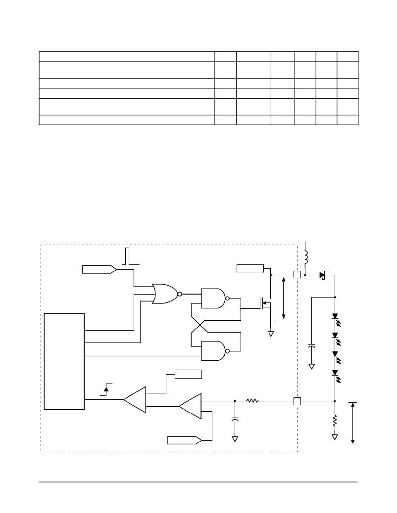
�DC/DC� OPERATION�
�The� DC/DC� converter� is� designed� to� supply� a� constant�
�current� to� the� external� load,� the� circuit� being� powered� from�
�a� standard� battery� supply.� Since� the� regulation� is� made� by�
�POR�
�means� of� a� current� loop,� the� output� voltage� will� varies�
�depending� upon� the� dynamic� impedance� presented� by� the�
�load.�
�Considering� high� intensity� LED,� the� output� voltage� can�
�range� from� a� low� 6.40� V� (two� LED� in� series� biased� with� a�
�low� current),� up� to� 21� V,� the� voltage� compliance� the� chip�
�can� sustain� continuously.�
�The� basic� DC/DC� structure� is� depicted� in� Figure� 3.� With�
�a� 28� V� maximum� rating� voltage� capability,� the� power�
�device� can� accommodate� high� voltage� source� without� any�
�leakage� current� downgrading.�
�V� bat�
�L1�
�22� m� H�
�Vd� sense�
�1�
�D1�
�TIME_OUT�
�Q1�
�Vds�
�LOGIC�
�CONTROL�
�ZERO_CROSSING�
�RESET�
�+�
�Vd� sense�
�R1�
�GND�
�GND�
�?�
�V(Ipeak)�
�?�
�+�
�C2�
�3�
�R2�
�xR�
�Vs�
�Vref�
�GND�
�Figure� 3.� Basic� DC/DC� Converter� Structure�
�http://onsemi.com�
�5�
�GND�
�相关PDF资料 |
PDF描述 |
|---|---|
| NCP5030MTTXGEVB | EVAL BOARD FOR NCP5030MTTXG |
| NCP5602EVB | EVAL BOARD FOR NCP5602 |
| NCP5603GEVB | EVAL BOARD FOR NCP5603G HI FREQ |
| NCP5604AAGEVB | EVAL BOARD FOR NCP5604AAG |
| NCP5608EVB | EVAL BOARD FOR NCP5608 |
相关代理商/技术参数 |
参数描述 |
|---|---|
| NCP5006SNT1 | 功能描述:LED照明驱动器 White LED Backlight RoHS:否 制造商:STMicroelectronics 输入电压:11.5 V to 23 V 工作频率: 最大电源电流:1.7 mA 输出电流: 最大工作温度: 安装风格:SMD/SMT 封装 / 箱体:SO-16N |
| NCP5006SNT1G | 功能描述:LED照明驱动器 White LED Backlight Boost RoHS:否 制造商:STMicroelectronics 输入电压:11.5 V to 23 V 工作频率: 最大电源电流:1.7 mA 输出电流: 最大工作温度: 安装风格:SMD/SMT 封装 / 箱体:SO-16N |
| NCP5007 | 制造商:ONSEMI 制造商全称:ON Semiconductor 功能描述:Compact Backlight LED Boost Driver |
| NCP5007/D | 制造商:未知厂家 制造商全称:未知厂家 功能描述:Compact Backlight LED Boost Driver |
| NCP5007_06 | 制造商:ONSEMI 制造商全称:ON Semiconductor 功能描述:Compact Backlight LED Boost Driver |
发布紧急采购,3分钟左右您将得到回复。