- 您现在的位置:买卖IC网 > PDF目录19327 > NCP500SN33T1 (ON Semiconductor)IC REG LDO 3.3V .15A 5TSOP PDF资料下载
参数资料
| 型号: | NCP500SN33T1 |
| 厂商: | ON Semiconductor |
| 文件页数: | 13/18页 |
| 文件大小: | 0K |
| 描述: | IC REG LDO 3.3V .15A 5TSOP |
| 产品变化通告: | Product Discontinuation 20/Aug/2008 |
| 标准包装: | 1 |
| 稳压器拓扑结构: | 正,固定式 |
| 输出电压: | 3.3V |
| 输入电压: | 最高 6V |
| 电压 - 压降(标准): | 0.15V @ 150mA |
| 稳压器数量: | 1 |
| 电流 - 输出: | 150mA |
| 工作温度: | -40°C ~ 85°C |
| 安装类型: | 表面贴装 |
| 封装/外壳: | 6-TSOP(0.059",1.50mm 宽)5 引线 |
| 供应商设备封装: | 5-TSOP |
| 包装: | 剪切带 (CT) |
| 其它名称: | NCP500SN33T1OSCT |
�� �
�
�NCP500,� NCV500�
�PD� +� J(max)�
�VinMAX� +� tot�
�The� maximum� dissipation� the� package� can� handle� is�
�given� by:�
�T� *� TA�
�R� q� JA�
�If� T� J� is� not� recommended� to� exceed� 125� ?� C,� then� the�
�NCP500� can� dissipate� up� to� 400� mW� @� 25� ?� C.�
�The� power� dissipated� by� the� NCP500� can� be� calculated�
�from� the� following� equation:�
�Ptot� +� Vin� *� Ignd� (Iout)� )� [Vin� *� Vout]� *� Iout�
�or�
�P� )� Vout * Iout�
�Ignd� )� Iout�
�If� a� 150� mA� output� current� is� needed� the� ground� current�
�is� extracted� from� the� data� sheet� curves:� 200� m� A� @� 150� mA.�
�For� a� NCP500SN18T1� (1.8� V),� the� maximum� input� voltage�
�will� then� be� 4.4� V,� good� for� a� 1� Cell� Li� ?� ion� battery.�
�Hints�
�Please� be� sure� the� V� in� and� GND� lines� are� sufficiently� wide.�
�When� the� impedance� of� these� lines� is� high,� there� is� a� chance�
�to� pick� up� noise� or� cause� the� regulator� to� malfunction.�
�Set� external� components,� especially� the� output� capacitor,�
�as� close� as� possible� to� the� circuit,� and� make� leads� as� short�
�as� possible.�
�Package� Placement�
�Component� pick� and� place� systems� are� composed� of� a� vision�
�system� that� recognizes� and� positions� the� component� and� a�
�mechanical� system� which� physically� performs� the� pick� and�
�place� operation.� Two� commonly� used� types� of� vision�
�systems� are:� (1)� a� vision� system� that� locates� a� package�
�silhouette� and� (2)� a� vision� system� that� locates� individual�
�bumps� on� the� interconnect� pattern.� The� latter� type� renders�
�more� accurate� place� but� tends� to� be� more� expensive� and� time�
�consuming.� Both� methods� are� acceptable� since� the� parts�
�align� due� to� a� self� ?� centering� feature� of� the� DFN� solder� joint�
�during� solder� re� ?� flow.�
�Solder� Paste�
�Type� 3� or� Type� 4� solder� paste� is� acceptable.�
�Re� ?� flow� and� Cleaning�
�The� DFN� may� be� assembled� using� standard� IR/IR�
�convection� SMT� re� ?� flow� processes� without� any� special�
�considerations.� As� with� other� packages,� the� thermal� profile�
�for� specific� board� locations� must� be� determined.� Nitrogen�
�purge� is� recommended� during� solder� for� no� ?� clean� fluxes.�
�The� DFN� is� qualified� for� up� to� three� re� ?� flow� cycles� at� 235� ?� C�
�peak� (J� ?� STD� ?� 020).� The� actual� temperature� of� the� DFN� is� a�
�function� of:�
�?� Component� density�
�?� Component� location� on� the� board�
�?� Size� of� surrounding� components�
�DFN� packages� can� be� placed� using� standard� pick� and�
�place� equipment� with� an� accuracy� of� "� 0.05� mm.�
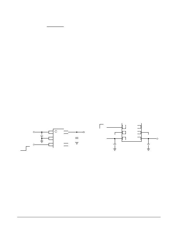
�ON�
�Battery� or�
�Unregulated�
�Voltage�
�ON�
�C1�
�+�
�1�
�2�
�3�
�5�
�4�
�+�
�V� out�
�C2�
�OFF�
�Battery� or�
�Unregulated�
�Voltage�
�+�
�C1�
�1�
�2�
�3�
�6�
�5�
�4�
�+�
�C2�
�V� out�
�OFF�
�Figure� 27.� Typical� Application� Circuit�
�http://onsemi.com�
�13�
�Figure� 28.� Typical� Application� Circuit�
�相关PDF资料 |
PDF描述 |
|---|---|
| ESC05DREH | CONN EDGECARD 10POS .100 EYELET |
| VJ1206A270JBCAT4X | CAP CER 27PF 200V 5% NP0 1206 |
| UMK325B7105MH-T | CAP CER 1UF 50V 20% X7R 1210 |
| GMM44DRKF-S13 | CONN EDGECARD 88POS .156 EXTEND |
| VI-BNR-CY-S | CONVERTER MOD DC/DC 7.5V 50W |
相关代理商/技术参数 |
参数描述 |
|---|---|
| NCP500SN33T1G | 功能描述:低压差稳压器 - LDO 3.3V 150mA CMOS w/Enable RoHS:否 制造商:Texas Instruments 最大输入电压:36 V 输出电压:1.4 V to 20.5 V 回动电压(最大值):307 mV 输出电流:1 A 负载调节:0.3 % 输出端数量: 输出类型:Fixed 最大工作温度:+ 125 C 安装风格:SMD/SMT 封装 / 箱体:VQFN-20 |
| NCP500SN33T1G | 制造商:ON Semiconductor 功能描述:IC, LDO VOLT REG, 3.3V, 150mA, TSOP-5 |
| NCP500SN33T1G-CUT TAPE | 制造商:ON 功能描述:NCP500 Series 3.3 V 150 mA CMOS Low Noise Low-Dropout Voltage Regulator-TSOP-5 |
| NCP500SN50T1 | 功能描述:低压差稳压器 - LDO 5.0V 150mA CMOS RoHS:否 制造商:Texas Instruments 最大输入电压:36 V 输出电压:1.4 V to 20.5 V 回动电压(最大值):307 mV 输出电流:1 A 负载调节:0.3 % 输出端数量: 输出类型:Fixed 最大工作温度:+ 125 C 安装风格:SMD/SMT 封装 / 箱体:VQFN-20 |
| NCP500SN50T1G | 功能描述:低压差稳压器 - LDO 5.0V 150mA CMOS w/Enable RoHS:否 制造商:Texas Instruments 最大输入电压:36 V 输出电压:1.4 V to 20.5 V 回动电压(最大值):307 mV 输出电流:1 A 负载调节:0.3 % 输出端数量: 输出类型:Fixed 最大工作温度:+ 125 C 安装风格:SMD/SMT 封装 / 箱体:VQFN-20 |
发布紧急采购,3分钟左右您将得到回复。