- 您现在的位置:买卖IC网 > PDF目录22239 > NCP500SQL33T1G (ON Semiconductor)IC REG LDO 3.3V .15A 6-DFN PDF资料下载
参数资料
| 型号: | NCP500SQL33T1G |
| 厂商: | ON Semiconductor |
| 文件页数: | 2/18页 |
| 文件大小: | 0K |
| 描述: | IC REG LDO 3.3V .15A 6-DFN |
| 标准包装: | 3,000 |
| 稳压器拓扑结构: | 正,固定式 |
| 输出电压: | 3.3V |
| 输入电压: | 最高 6V |
| 电压 - 压降(标准): | 0.15V @ 150mA |
| 稳压器数量: | 1 |
| 电流 - 输出: | 150mA |
| 工作温度: | -40°C ~ 85°C |
| 安装类型: | 表面贴装 |
| 封装/外壳: | 6-VDFN 裸露焊盘 |
| 供应商设备封装: | 6-DFN(2x2.2) |
| 包装: | 带卷 (TR) |
| 其它名称: | NCP500SQL33T1GOS |
�� �
�
�NCP500,� NCV500�
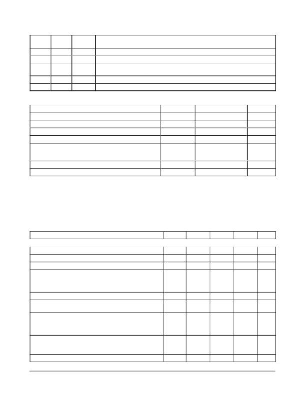
�PIN� FUNCTION� DESCRIPTION�
�TSOP� ?� 5�
�DFN� 2x2�
�Pin� No.�
�1�
�2�
�3�
�4�
�5�
�Pin� No.�
�3�
�2,� 5�
�1�
�6�
�4�
�Pin� Name�
�V� in�
�GND�
�Enable�
�N/C�
�V� out�
�Description�
�Positive� power� supply� input� voltage.�
�Power� supply� ground.�
�This� input� is� used� to� place� the� device� into� low� ?� power� standby.� When� this� input� is� pulled� to� a� logic�
�low,� the� device� is� disabled.� If� this� function� is� not� used,� Enable� should� be� connected� to� V� in� .�
�No� internal� connection.�
�Regulated� output� voltage.�
�MAXIMUM� RATINGS�
�Rating�
�Input� Voltage�
�Enable� Voltage�
�Output� Voltage�
�Output� Short� Circuit� Duration�
�Thermal� Resistance,� Junction� ?� to� ?� Ambient�
�TSOP� ?� 5�
�DFN� (Note� 3)�
�Operating� Junction� Temperature�
�Storage� Temperature�
�Symbol�
�V� in�
�V� on/off�
�V� out�
�?�
�R� q� JA�
�T� J�
�T� stg�
�Value�
�0� to� 6.0�
�?� 0.3� to� V� in� +0.3�
�?� 0.3� to� V� in� +0.3�
�Infinite�
�250�
�225�
�+125�
�?� 65� to� +150�
�Unit�
�V�
�V�
�V�
�?�
�?� C/W�
�?� C�
�?� C�
�Stresses� exceeding� Maximum� Ratings� may� damage� the� device.� Maximum� Ratings� are� stress� ratings� only.� Functional� operation� above� the�
�Recommended� Operating� Conditions� is� not� implied.� Extended� exposure� to� stresses� above� the� Recommended� Operating� Conditions� may� affect�
�device� reliability.�
�1.� This� device� series� contains� ESD� protection� and� exceeds� the� following� tests:�
�Human� Body� Model� 2000� V� per� MIL� ?� STD� ?� 883,� Method� 3015�
�Machine� Model� Method� 200� V� Latch� up� capability� (85� ?� C)� "� 100� mA.�
�2.� Device� is� internally� limited� to� 160� ?� C� by� thermal� shutdown.�
�3.� For� more� information,� refer� to� application� note,� AND8080/D.�
�ELECTRICAL� CHARACTERISTICS� (V� in� =� 2.35� V,� C� in� =� 1.0� m� F,� C� out� =� 1.0� m� F,� for� typical� value� T� A� =� 25� ?� C,� for� min� and�
�max� values� T� A� =� ?� 40� ?� C� to� 85� ?� C,� T� jmax� =� 125� ?� C,� unless� otherwise� noted)�
�Characteristic�
�Symbol�
�Min�
�Typ�
�Max�
�Unit�
�?� 1.8� V�
�Output� Voltage� (T� A� =� ?� 40� ?� C� to� 85� ?� C,� I� out� =� 1.0� mA� to� 150� mA)�
�Line� Regulation� (V� in� =� 2.3� V� to� 6.0� V,� I� out� =� 1.0� mA)�
�Load� Regulation� (I� out� =� 1.0� mA� to� 150� mA)�
�Dropout� Voltage� (Measured� at� V� out� ?� 2.0%,� T� A� =� ?� 40� ?� C� to� 85� ?� C)�
�(Iout� =� 1.0� mA)�
�(Iout� =� 75� mA)�
�(Iout� =� 150� mA)�
�Output� Short� Circuit� Current�
�Ripple� Rejection�
�V� out�
�Reg� line�
�Reg� load�
�V� in� ?� V� out�
�I� out(max)�
�RR�
�1.755�
�?�
�?�
�?�
�?�
�?�
�200�
�?�
�1.8�
�1.0�
�15�
�2.0�
�140�
�270�
�540�
�62�
�1.845�
�10�
�45�
�10�
�200�
�350�
�700�
�?�
�V�
�mV�
�mV�
�mV�
�mA�
�dB�
�(V� in� =� V� out� (nom.)� +� 1.0� V� +� 0.5� V� pp� ,� f� =� 1.0� kHz,� I� o� =� 60� mA)�
�Quiescent� Current�
�(Enable� Input� =� 0� V)�
�(Enable� Input� =� 0.9� V,� I� out� =� 1.0� mA)�
�(Enable� Input� =� 0.9� V,� I� out� =� 150� mA)�
�Enable� Input� Threshold� Voltage�
�(Voltage� Increasing,� Output� Turns� On,� Logic� High)�
�(Voltage� Decreasing,� Output� Turns� Off,� Logic� Low)�
�Enable� Input� Bias� Current�
�I� Q�
�V� th(EN)�
�I� IB(EN)�
�?�
�?�
�?�
�0.9�
�?�
�?�
�0.01�
�175�
�175�
�?�
�?�
�3.0�
�1.0�
�300�
�300�
�?�
�0.15�
�100�
�m� A�
�V�
�nA�
�http://onsemi.com�
�2�
�相关PDF资料 |
PDF描述 |
|---|---|
| 395-130-542-201 | CARD EDGE 130PS DL .100X.200 BLK |
| ABE25DHRR | CONN CARD EXTEND 50POS 1MM SLD |
| 395-130-541-804 | CARD EDGE 130PS DL .100X.200 BLK |
| T86C155M050ESSS | CAP TANT 1.5UF 50V 20% 2312 |
| NCP500SQL30T1G | IC REG LDO 3V .15A 6-DFN |
相关代理商/技术参数 |
参数描述 |
|---|---|
| NCP500SQL50T1 | 功能描述:低压差稳压器 - LDO 5.0V 150mA CMOS RoHS:否 制造商:Texas Instruments 最大输入电压:36 V 输出电压:1.4 V to 20.5 V 回动电压(最大值):307 mV 输出电流:1 A 负载调节:0.3 % 输出端数量: 输出类型:Fixed 最大工作温度:+ 125 C 安装风格:SMD/SMT 封装 / 箱体:VQFN-20 |
| NCP500SQL50T1G | 功能描述:低压差稳压器 - LDO 5.0V 150mA CMOS w/Enable RoHS:否 制造商:Texas Instruments 最大输入电压:36 V 输出电压:1.4 V to 20.5 V 回动电压(最大值):307 mV 输出电流:1 A 负载调节:0.3 % 输出端数量: 输出类型:Fixed 最大工作温度:+ 125 C 安装风格:SMD/SMT 封装 / 箱体:VQFN-20 |
| NCP5010 | 制造商:ONSEMI 制造商全称:ON Semiconductor 功能描述:500 mW Boost Converter for White LEDs |
| NCP5010_06 | 制造商:ONSEMI 制造商全称:ON Semiconductor 功能描述:500 mW Boost Converter for White LEDs |
| NCP5010EVB | 功能描述:电源管理IC开发工具 EVAL BRD FOR NCP5010FCT1G RoHS:否 制造商:Maxim Integrated 产品:Evaluation Kits 类型:Battery Management 工具用于评估:MAX17710GB 输入电压: 输出电压:1.8 V |
发布紧急采购,3分钟左右您将得到回复。