- 您现在的位置:买卖IC网 > PDF目录20796 > NCP5030MTTXG (ON Semiconductor)IC LED DVR HIGH BRIGHT 12WDFN PDF资料下载
参数资料
| 型号: | NCP5030MTTXG |
| 厂商: | ON Semiconductor |
| 文件页数: | 10/14页 |
| 文件大小: | 0K |
| 描述: | IC LED DVR HIGH BRIGHT 12WDFN |
| 标准包装: | 1 |
| 恒定电流: | 是 |
| 拓扑: | PWM,降压(降压),升压(升压) |
| 输出数: | 1 |
| 内部驱动器: | 是 |
| 类型 - 主要: | 闪灯/白光 |
| 类型 - 次要: | 白色 LED |
| 频率: | 600kHz ~ 800kHz |
| 电源电压: | 2.7 V ~ 5.5 V |
| 输出电压: | 2.2 V ~ 5.5 V |
| 安装类型: | 表面贴装 |
| 封装/外壳: | 12-WFDFN 裸露焊盘 |
| 供应商设备封装: | 12-WDFN(4x3) |
| 包装: | 标准包装 |
| 工作温度: | -40°C ~ 85°C |
| 其它名称: | NCP5030MTTXGOSDKR |
�� �
�
�NCP5030�
�the� inductor� is� charged� by� current� from� the� battery� to� store�
�up� energy.� During� this� phase� the� switch� N2� is� on� and� P2� is�
�off.� The� switch� current� is� measured� by� the� SENSE�
�CURRENT� and� added� to� the� RAMP� COMP� signal.� Then�
�PWM� COMP� compares� the� output� of� the� adder� and� the�
�signal� from� ERROR� AMP.� When� the� comparator� threshold�
�is� exceeded,� the� flip� ?� flop� circuit� is� reset,� P2� switch� is�
�turned� on,� and� N2� is� off� until� the� rising� edge� of� the� next�
�LX1�
�V� IN�
�Start�
�Cycle�
�clock� cycle.�
�LX2�
�V� OUT�
�1.43� m� S�
�I� peak�
�LX1�
�LX2�
�Start�
�Cycle�
�1.43� m� S�
�LX1� =� V� IN�
�I� peak�
�I� L�
�I� OUT�
�T� ON� T� OFF�
�T� C�
�I� valley�
�I� L�
�T� ON�
�T� OFF�
�I� valley�
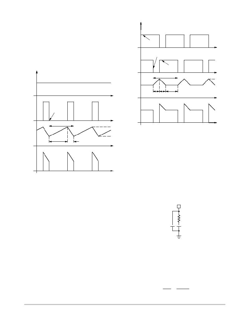
�Figure� 20.� Basic� DC� ?� DC� BB� Operation�
�In� addition,� there� are� four� safety� circuits� like� OVP,�
�UVLO,� IPEAK� COMP,� THERMAL� PROTECTION,�
�which� can� disable� the� DC� ?� DC� conversion.�
�Error� Amp� and� Compensation�
�I� OUT�
�Figure� 19.� Basic� DC� ?� DC� Boost� Operation�
�Buck� ?� Boost� Mode�
�(V� IN� –� 650� mV� <� V� OUT� <� V� IN� +� 375� mV)�
�Figure� 20� shows� the� basic� DC� ?� DC� Buck� ?� Boost�
�operation.� Now,� all� four� switches� are� running� and� the�
�controller� operates� in� three� separate� phases� to� reach� higher�
�efficiency.� The� first� step� is� T� ON� when� the� inductor� is�
�charged� by� current� from� the� battery.� During� this� phase� the�
�switch� P1_N2� are� on� and� P2_N1� are� off.� Like� the� other�
�Regulation� loop� is� closed� by� the� error� amplifier,� which�
�compares� the� feedback� voltage� with� the� reference� set� at�
�200� mV.� Thanks� to� the� transconductance� structure,� the�
�compensation� network� is� directly� connected� to� the� error�
�amplifier� output.� This� external� passive� network� is�
�necessary� to� sets� the� dominant� pole� to� gets� a� good� loop�
�stability.� The� compensation� network� shown� in� Figure� 21�
�provides� a� phase� margin� greater� than� 45� °� whatever� the�
�current� drives� in� a� white� LED� load.�
�COMP�
�100� k�
�modes,� the� current� measured� by� SENSE� CURRENT� is�
�added� to� the� RAMP� COMP� signal� and� compared� by� PWM�
�COMP� with� the� signal� from� ERROR� AMP.� When� PWM�
�22� pF�
�330� pF�
�RSENSE� +�
�+� 250� m� W�
�+�
�ILED�
�800� mA�
�COMP� threshold� is� exceeded,� the� flip� ?� flop� circuit� is� reset�
�and� the� controller� switches� in� T� OFF� phase.� In� this� second�
�phase,� the� switch� P1_N2� are� off� and� P2_N1� are� ON.�
�Because� time� of� T� OFF� phase� is� constant,� the� current� stored�
�in� the� inductor� during� 250� ns� (nominal)� is� drained� to� V� OUT� .�
�After� this,� CONSTANT� T� OFF� delay� is� over,� the� circuit� logic�
�switches� in� the� third� phase� named� TC� (Time� Conduction)�
�where� the� inductor� is� directly� connected� from� PVIN� to�
�V� OUT� .� The� switch� P1_P2� are� on� and� switches� N_N2� are� off�
�until� the� rising� edge� of� the� next� clock� cycle.�
�Figure� 21.� Compensation� Network�
�LED� Current� Selection�
�The� feedback� resistor� (R� SENSE� )� determines� the� LED�
�current� in� steady� state.� The� control� loop� regulates� the�
�current� in� such� a� way� that� the� average� voltage� at� the� FB�
�input� is� 200� mV� (nominal).� For� example,� should� one� need�
�800� mA� output� current,� R� SENSE� should� be� selected�
�according� to� the� following� equation:�
�FBV 200 mV�
�(eq.� 1)�
�http://onsemi.com�
�10�
�相关PDF资料 |
PDF描述 |
|---|---|
| USR 2-0808 10K OHM D 0.01% 1PPM | RES 10K OHM .6W .01% FOIL RADIAL |
| USR 2-0808 100 OHM D 0.01% 1PPM | RES 100 OHM .6W .01% FOIL RADIAL |
| REC8-2415SRWZ/H2/A/M | CONV DC/DC 8W 24VIN 15VOUT |
| P51-1500-S-G-MD-5V-000-000 | SENSOR 1500PSIS 1/8 NPT 5V MINI |
| REC5-1209SRW/H4/A/SMD/CTRL-R | CONV DC/DC 5W 9-18VIN 09VOUT |
相关代理商/技术参数 |
参数描述 |
|---|---|
| NCP5030MTTXGEVB | 功能描述:电源管理IC开发工具 NCP5030MTTXG EVAL BRD RoHS:否 制造商:Maxim Integrated 产品:Evaluation Kits 类型:Battery Management 工具用于评估:MAX17710GB 输入电压: 输出电压:1.8 V |
| NCP5030MTTXGEVB | 制造商:ON Semiconductor 功能描述:NCP5030MTTXG EVAL BOARD ;ROHS COMPLIANT: NO |
| NCP5050 | 制造商:ONSEMI 制造商全称:ON Semiconductor 功能描述:4.5 W Flash White LED Boost Driver |
| NCP5050 AW37A WAF | 制造商:ON Semiconductor 功能描述: |
| NCP5050GEVB | 功能描述:LED 照明开发工具 NCV8925 EVAL BRD RoHS:否 制造商:Fairchild Semiconductor 产品:Evaluation Kits 用于:FL7732 核心: 电源电压:120V 系列: 封装: |
发布紧急采购,3分钟左右您将得到回复。