- 您现在的位置:买卖IC网 > PDF目录16918 > NCP508SQ15T1GEVB (ON Semiconductor)BOARD EVALUATION NCP507 1.5V PDF资料下载
参数资料
| 型号: | NCP508SQ15T1GEVB |
| 厂商: | ON Semiconductor |
| 文件页数: | 2/15页 |
| 文件大小: | 0K |
| 描述: | BOARD EVALUATION NCP507 1.5V |
| 设计资源: | NCP508SQ15T1GEVB Schematic NCP508SQ15T1GEVB Gerber Files NCP508SQ15T1GEVB Bill of Materials |
| 标准包装: | 1 |
| 每 IC 通道数: | 1 - 单 |
| 输出电压: | 1.5V |
| 电流 - 输出: | 50mA |
| 输入电压: | 5V |
| 稳压器类型: | 正,固定式 |
| 工作温度: | -40°C ~ 85°C |
| 板类型: | 完全填充 |
| 已供物品: | 板 |
| 已用 IC / 零件: | NCP508 |
| 其它名称: | NCP508SQ15T1GEVBOS |
��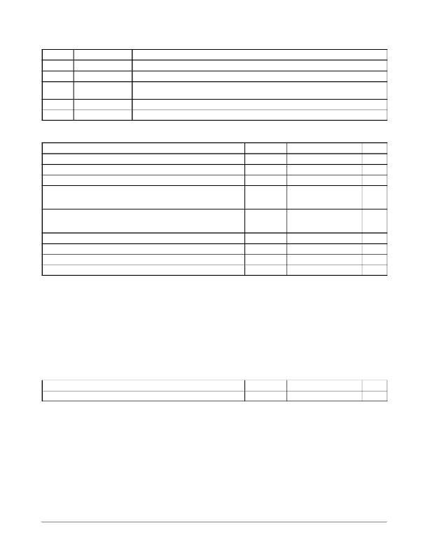 �
�
�NCP508�
�PIN� FUNCTION� DESCRIPTION�
�Pin� No.�
�1�
�2�
�3�
�4�
�5�
�Pin� Name�
�V� in�
�GND�
�Enable�
�N/C�
�V� out�
�Description�
�Positive� power� supply� input� voltage�
�Power� supply� ground�
�This� input� is� used� to� place� the� device� into� low� ?� power� stand� by.� When� this� input� is� pulled� low,� the�
�device� is� disabled.� If� this� function� is� not� used,� Enable� should� be� connected� to� V� in� .�
�Not� connected� pin�
�Regulated� output� voltage�
�MAXIMUM� RATING�
�Rating�
�Input� Voltage�
�Enable� Voltage�
�Output� Voltage�
�Power� Dissipation� and� Thermal� Characteristics� (SC� ?� 88A)�
�Power� Dissipation�
�Thermal� Resistance,� Junction� ?� to� ?� Ambient� (Note� 4)�
�Power� Dissipation� and� Thermal� Characteristics� (WDFN6)�
�Power� Dissipation�
�Thermal� Resistance,� Junction� ?� to� ?� Ambient� (Note� 4)�
�Maximum� Junction� Temperature�
�Operating� Ambient� Temperature�
�Storage� Temperature�
�Lead� Soldering� Temperature� @� 260� °� C�
�Symbol�
�V� in(max)�
�Enable�
�V� out�
�P� D�
�R� q� JA�
�P� D�
�R� q� JA�
�T� J�
�T� A�
�T� stg�
�T� solder�
�Value�
�13.0�
�?� 0.3� to� V� in(max)� +� 0.3�
�?� 0.3� to� V� in(max)� +� 0.3�
�Internally� Limited�
�200�
�Internally� Limited�
�313�
�+125�
�?� 40� to� +85�
�?� 55� to� +150�
�10�
�Unit�
�V�
�V�
�V�
�W�
�°� C/W�
�W�
�°� C/W�
�°� C�
�°� C�
�°� C�
�sec�
�Stresses� exceeding� Maximum� Ratings� may� damage� the� device.� Maximum� Ratings� are� stress� ratings� only.� Functional� operation� above� the�
�Recommended� Operating� Conditions� is� not� implied.� Extended� exposure� to� stresses� above� the� Recommended� Operating� Conditions� may� affect�
�device� reliability.�
�1.� This� device� series� contains� ESD� protection� and� exceeds� the� following� tests:�
�Human� Body� Model� 2000� V� per� MIL� ?� STD� ?� 883,� Method� 3015.�
�Machine� Model� Method� 200� V�
�2.� Latch� up� Capability� (85� °� C)� $� 100� mA� DC� with� trigger� voltage�
�3.� Maximum� package� power� dissipation� limits� must� be� observed.�
�P� D� +�
�T� J� (� max� )� *� T� A�
�R� q� JA�
�4.� R� q� JA� on� a� 30� x� 30� mm� PCB� Cu� thickness� 1� oz;� T� A� =� 25� °� C.�
�RECOMMENDED� OPERATING� CONDITIONS�
�Maximum� Operating� Input� Voltage�
�Rating�
�Symbol�
�V� in�
�Max�
�7.0�
�Unit�
�V�
�http://onsemi.com�
�2�
�相关PDF资料 |
PDF描述 |
|---|---|
| MLG0603S9N1J | INDUCTOR MULTILAYER 9.1NH 0201 |
| EEM18DSEF | CONN EDGECARD 36POS .156 EYELET |
| 820243-000 | BOOT MOLDED |
| 3-1589476-7 | CONN RCPT 65POS 30AWG 12IN |
| 811933-000 | BOOT MOLDED STR SIZE 42 W/LIP |
相关代理商/技术参数 |
参数描述 |
|---|---|
| NCP508SQ18T1G | 功能描述:低压差稳压器 - LDO LDO RoHS:否 制造商:Texas Instruments 最大输入电压:36 V 输出电压:1.4 V to 20.5 V 回动电压(最大值):307 mV 输出电流:1 A 负载调节:0.3 % 输出端数量: 输出类型:Fixed 最大工作温度:+ 125 C 安装风格:SMD/SMT 封装 / 箱体:VQFN-20 |
| NCP508SQ25T1G | 功能描述:低压差稳压器 - LDO LDO RoHS:否 制造商:Texas Instruments 最大输入电压:36 V 输出电压:1.4 V to 20.5 V 回动电压(最大值):307 mV 输出电流:1 A 负载调节:0.3 % 输出端数量: 输出类型:Fixed 最大工作温度:+ 125 C 安装风格:SMD/SMT 封装 / 箱体:VQFN-20 |
| NCP508SQ28T1G | 功能描述:低压差稳压器 - LDO LDO RoHS:否 制造商:Texas Instruments 最大输入电压:36 V 输出电压:1.4 V to 20.5 V 回动电压(最大值):307 mV 输出电流:1 A 负载调节:0.3 % 输出端数量: 输出类型:Fixed 最大工作温度:+ 125 C 安装风格:SMD/SMT 封装 / 箱体:VQFN-20 |
| NCP508SQ30T1G | 功能描述:低压差稳压器 - LDO LDO RoHS:否 制造商:Texas Instruments 最大输入电压:36 V 输出电压:1.4 V to 20.5 V 回动电压(最大值):307 mV 输出电流:1 A 负载调节:0.3 % 输出端数量: 输出类型:Fixed 最大工作温度:+ 125 C 安装风格:SMD/SMT 封装 / 箱体:VQFN-20 |
| NCP508SQ33T1G | 功能描述:低压差稳压器 - LDO LDO RoHS:否 制造商:Texas Instruments 最大输入电压:36 V 输出电压:1.4 V to 20.5 V 回动电压(最大值):307 mV 输出电流:1 A 负载调节:0.3 % 输出端数量: 输出类型:Fixed 最大工作温度:+ 125 C 安装风格:SMD/SMT 封装 / 箱体:VQFN-20 |
发布紧急采购,3分钟左右您将得到回复。