参数资料
| 型号: | NCP5203MNR2 |
| 厂商: | ON Semiconductor |
| 文件页数: | 7/10页 |
| 文件大小: | 0K |
| 描述: | IC CTRLR PWR DDR DUAL 5X6 18-DFN |
| 产品变化通告: | Product Obsolescence 30/Sept/2009 |
| 标准包装: | 2,500 |
| 应用: | 控制器,DDR |
| 输入电压: | 4.5 V ~ 5.5 V |
| 输出数: | 2 |
| 工作温度: | 0°C ~ 70°C |
| 安装类型: | 表面贴装 |
| 封装/外壳: | 18-VFDFN 裸露焊盘 |
| 供应商设备封装: | 18-DFN(5x6) |
| 包装: | 带卷 (TR) |
| 其它名称: | NCP5203MNR2OS |
�� �
�
�NCP5203�
�DETAILED� OPERATING� DESCRIPTION�
�General�
�The� NCP5203� 2?in?1� DDR� Power� Controller� combines�
�the� efficiency� of� a� VDDQ� PWM� controller� with� the�
�simplicity� of� a� linear� regulator� for� VTT� termination.� Both�
�VDDQ� and� VTT� outputs� can� be� user� adjusted.�
�The� inclusion� of� both� VDDQ� and� VTT� power� good�
�voltage� monitors,� soft?start,� VDDQ� overvoltage� and�
�undervoltage� detection,� supply� undervoltage� monitors,� and�
�thermal� shutdown,� makes� this� device� a� total� power� solution�
�for� high� current� DDR� memory� systems.�
�VDDQ� Switching� Regulator� in� Normal� (S0)� Mode�
�The� VDDQ� regulator� is� a� switching� synchronous�
�rectification� buck� controller� directly� driving� two� external�
�N?Channel� power� FETs.� An� external� resistor� divider� sets�
�the� nominal� output� voltage.� The� control� architecture� is�
�voltage� mode� fixed� frequency� PWM� (300� kHz� ±� 12.5%)�
�with� external� compensation.� The� VDDQ� output� voltage� is�
�divided� down� and� fed� back� to� the� inverting� input� of� an�
�internal� amplifier� through� the� FBDDQ� pin� to� close� the� loop�
�at� VDDQ� =� VFBDDQ� � (1� +� R2/R1).� This� amplifier�
�compares� the� feedback� voltage� with� an� internal� VREF1�
�(=� 1.25� V)� to� generate� an� error� signal� for� the� PWM�
�comparator.� This� error� signal� is� further� compared� with� a�
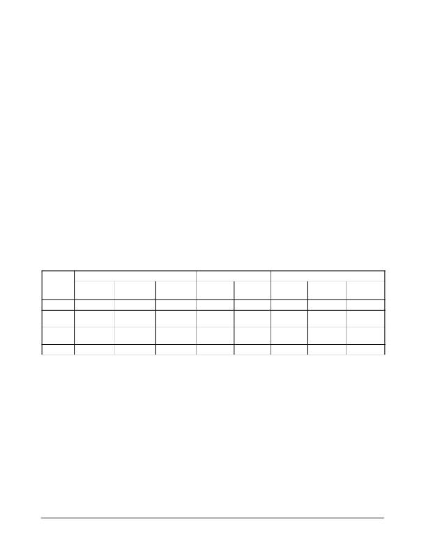
�Table� 1.� State,� Operation,� Input� and� Output� Condition� Table�
�fixed� frequency� Ramp� waveform� derived� from� the� internal�
�oscillator� to� generate� a� pulse?width?modulated� signal.�
�This� PWM� signal� drives� the� external� N?Channel� Power�
�FETs� via� the� TGDDQ� and� BGDDQ� pins.� External� inductor�
�L� and� capacitor� COUT1� filter� the� output.� The� VDDQ�
�output� voltage� ramps� up� at� a� pre?defined� soft?start� rate�
�each� time� the� IC� exits� S5.� When� in� normal� mode,� and�
�regulation� of� VDDQ� is� detected,� signal� INREGDDQ� will�
�go� high� to� notify� the� control� logic� block.�
�For� enhanced� efficiency,� an� active� synchronous� switch� is�
�used� to� eliminate� the� conduction� loss� contributed� by� the�
�forward� voltage� of� a� diode� or� Schottky� diode� rectifier.�
�Adaptive� non?overlap� timing� control� of� the�
�complementary� gate� drive� output� signals� is� provided� to�
�reduce� shoot?through� current.�
�Tolerance� of� VDDQ�
�The� tolerance� of� VFBDDQ� and� the� ratio� of� the� external�
�resistor� divider� R2/R1� both� impact� the� precision� of� VDDQ.�
�When� the� control� loop� is� in� regulation,� VDDQ� =� VFBDDQ�
�� (1� +� R2/R1).� With� a� worst� case� (overtemperature)�
�VFBDDQ� tolerance� of� ±� 2%,� a� worst� case� range� of� 2.5%� for�
�VDDQ� will� be� assured� if� the� ratio� R2/R1� is� specified� as�
�0.98985� ±� 1%.�
�5VDUAL�
�USER� INPUTS�
�OPERATING� CONDITIONS�
�OUTPUT� CONDITIONS�
�MODE�
�S5�
�S0�
�UVLO�
�Low�
�High�
�VDDQEN�
�X�
�High�
�VTTEN�
�X�
�High�
�VDDQ�
�H?Z�
�Normal�
�VTT�
�H?Z�
�Normal�
�TGDDQ�
�Low�
�Normal�
�BGDDQ�
�Low�
�Normal�
�PGOOD�
�Low�
�H?Z�
�(300� kHz)�
�(300� kHz)�
�S3�
�High�
�High�
�Low�
�Standby�
�H?Z�
�Normal�
�Low�
�Low�
�(600� kHz)�
�S5�
�High�
�Low�
�X�
�H?Z�
�H?Z�
�Low�
�Low�
�Low�
�VDDQ� Regulator� in� Standby� Mode� (S3)�
�During� S3,� the� VDDQ� regulator� operates� in�
�asynchronous� switch� mode.� The� switching� frequency� is�
�increased� to� 600� kHz,� the� low?side� FET� is� disabled,� and� the�
�body� diode� of� the� low� side� FET� is� used.� The� regulator� will�
�operate� in� discontinuous� conduction� mode� (DCM)� and� the�
�switching� frequency� is� doubled� to� reduce� peak� conduction�
�current.�
�VDDQ� Regulator� Fault� Protection�
�During� S0� and� S3,� the� external� resistor� (RL1)� sets� the�
�current� limit� for� the� high?side� switch.� An� internal� 35� m� A�
�across� this� resistor.� This� voltage� is� compared� to� the� voltage�
�at� SWDDQ� pin� when� the� TGDDQ� is� high� after� a� fixed�
�blanking� period� of� 500� ns� to� avoid� false� current� limit�
�triggering.� When� the� voltage� at� SWDDQ� is� lower� than�
�OCDDQ,� an� overcurrent� condition� occurs,� upon� which� all�
�outputs� will� be� latched� off� to� protect� against� a�
�short?to?ground� condition� on� SWDDQ� or� VDDQ.� The� IC�
�will� be� reset� once� 5VDUAL� or� VDDQEN� is� cycled.�
�VDDQ� Regulator� Feedback� Compensation�
�The� recommended� compensation� network� is� shown� in�
�Figure� 2.�
�current� sink� at� OCDDQ� pin� establishes� a� voltage� drop�
�http://onsemi.com�
�7�
�相关PDF资料 |
PDF描述 |
|---|---|
| X4323V8I | IC SUPERVISOR CPU 32K EE 8-TSSOP |
| NCP5201MNR2 | IC CTRLR PWR DDR DUAL 5X6 18-DFN |
| HSM24DRYN-S13 | CONN EDGECARD 48POS .156 EXTEND |
| HBC35DRTI-S13 | CONN EDGECARD 70POS .100 EXTEND |
| HMM24DRYN-S13 | CONN EDGECARD 48POS .156 EXTEND |
相关代理商/技术参数 |
参数描述 |
|---|---|
| NCP5203MNR2G | 功能描述:DC/DC 开关控制器 2-in-1 DDR Power RoHS:否 制造商:Texas Instruments 输入电压:6 V to 100 V 开关频率: 输出电压:1.215 V to 80 V 输出电流:3.5 A 输出端数量:1 最大工作温度:+ 125 C 安装风格: 封装 / 箱体:CPAK |
| NCP5208 | 制造商:ONSEMI 制造商全称:ON Semiconductor 功能描述:DDR−I/II Termination Regulator |
| NCP5208/D | 制造商:ONSEMI 制造商全称:ON Semiconductor 功能描述:DDR-I/II Termination Regulator |
| NCP5208_06 | 制造商:ONSEMI 制造商全称:ON Semiconductor 功能描述:DDR−I/II Termination Regulator |
| NCP5208DR2 | 功能描述:线性稳压器 - 标准 DDR-I/II Termination RoHS:否 制造商:STMicroelectronics 输出类型: 极性: 输出电压:1.8 V 输出电流:150 mA 负载调节: 最大输入电压:5.5 V 线路调整率: 最大工作温度:+ 125 C 安装风格:SMD/SMT 封装 / 箱体:SOT-323-5L |
发布紧急采购,3分钟左右您将得到回复。