- 您现在的位置:买卖IC网 > Datasheet目录996 > NCP5604AAGEVB (ON Semiconductor)EVAL BOARD FOR NCP5604AAG Datasheet资料下载
参数资料
| 型号: | NCP5604AAGEVB |
| 厂商: | ON Semiconductor |
| 文件页数: | 10/15页 |
| 文件大小: | 0K |
| 描述: | EVAL BOARD FOR NCP5604AAG |
| 产品变化通告: | Product Obsolescence 30/Jun/2011 |
| 设计资源: | NCP5604A EVB BOM NCP5604AAGEVB Gerber Files NCP5604 EVB Schematic NCP5604 Demo Brd BOM |
| 标准包装: | 1 |
| 电流 - 输出 / 通道: | 100mA |
| 输出及类型: | 4,非隔离 |
| 输出电压: | 4.8 ~ 6 V |
| 特点: | 通-断开关 |
| 输入电压: | 2.85 ~ 5.5 V |
| 已供物品: | 板 |
| 已用 IC / 零件: | NCP5604 |
| 其它名称: | NCP5604AAGEVBOS |
�� �
�
�NCP5604A,� NCP5604B�
�Vbat�
�220� nF/10� V�
�Input� PWM� Signal� Frequency:�
�100� Hz� to� 200� kHz�
�GND�
�C4�
�C3�
�1�
�VBAT�
�C2P�
�4.7uF/6.3V�
�1�
�VBAT�
�C2N�
�14�
�U1�
�CONTROL�
�GND�
�R1�
�100k�
�2�
�3�
�4�
�EN�
�IREF� NCP5604B�
�AGND�
�C2P�
�C1P�
�13�
�11�
�C2�
�220� nF/10� V�
�C1�
�PWM�
�2�
�3�
�EN�
�IREF�
�C2N�
�C3P�
�9�
�PGND�
�C1N�
�VOUT�
�10�
�12�
�220� nF/10� V�
�C3N�
�D2�
�D1�
�LWY87S�
�C5�
�GND�
�4�
�9�
�AGND�
�PGND�
�VOUT�
�D3�
�LWY87S�
�LWY87S�
�GND�
�GND�
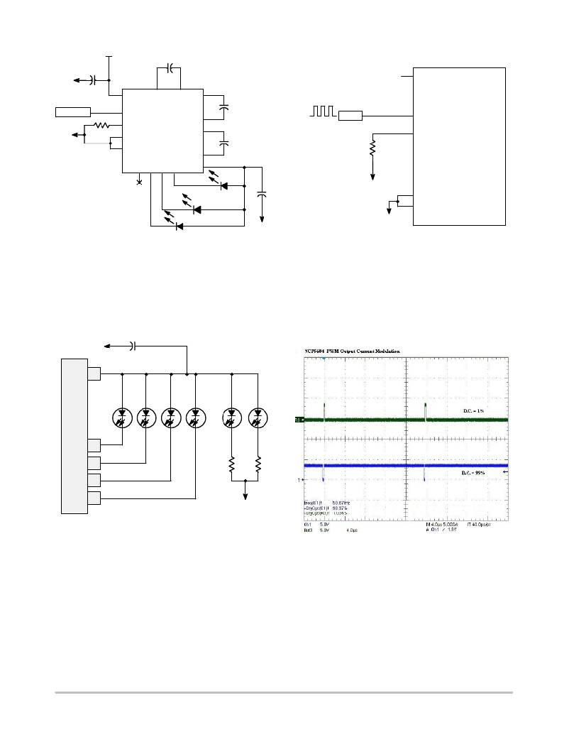
�Figure� 9.� Using� the� NCP5604B� to� Drive� a� Three� LED�
�Figure� 11.� Basic� Digital� PWM� Dimming� Control�
�Layout�
�The� PWM� frequency� can� be� up� to� 200� kHz� once� the�
�Finally,� an� external� network� can� be� connected� across�
�Vout� and� ground,� but� the� current� through� such� network� will�
�not� be� regulated� by� the� NCP5604A� chip� (see� Figure� 10).�
�On� top� of� that,� the� total� current� out� of� the� Vout� pin� shall� be�
�limited� to� 100� mA.�
�circuit� has� been� properly� started.� On� the� other� hand,� with�
�a� 1%� to� 99%� span,� the� circuit� supports� a� large� Duty� Cycle�
�to� accommodate� any� range� of� dimming.� The� waveforms�
�given� in� Figure� 12� illustrate� the� NCP5604A� behavior�
�during� the� 50� kHz� PWM� operation.� The� same� mechanism�
�applies� for� the� NCP5604B� version.�
�GND�
�C5�
�1� m� F/6.3� V�
�12�
�8�
�7�
�6�
�5�
�GND�
�Figure� 10.� Extra� Load� Connected� to� Vout�
�DIMMING�
�The� dimming� can� be� achieved� by� two� means:�
�?� Use� a� digital� PWM� signal� to� control� the� EN� pin�
�?� Use� an� analog� signal� to� control� the� reference� current�
�IREF� pin.�
�The� digital� PWM� is� straightforward,� yielding� a� zero� to�
�100%� duty� cycle,� but� the� output� current� is� pulsed� since� the�
�system� is� continuously� switched� ON/OFF.� There� is� no� need�
�for� extra� passive� component,� the� clock� being� provided� by�
�an� I/O� port� from� the� MCU� (see� Figure� 11).�
�Figure� 12.� PWM� Modulation� Span:� 1%� to� 99%�
�Besides� the� popular� PWM� mode,� a� simple� analog�
�technique� can� be� built� with� two� extra� components� (one�
�resistor� +� one� NMOS),� the� net� advantage� being� a�
�continuous� output� current� once� the� operating� point� has�
�been� stabilized� (see� Figure� 13).� The� absolute� output�
�current� tolerance� depends� upon� the� precision� of� the� two�
�external� resistors,� the� R� DS(on)� of� the� NMOS� being�
�negligible� in� front� of� the� resistor� value.� The� example� given,�
�Figure� 13� yields� a� 1.0� mA� output� current� when� Q1� is� OFF,�
�http://onsemi.com�
�10�
�相关PDF资料 |
PDF描述 |
|---|---|
| NCP5608EVB | EVAL BOARD FOR NCP5608 |
| NCP5612GEVB | EVAL BOARD FOR NCP5612G |
| NCV7680PWR22GEVB | BOARD EVALUATION NCV7680 |
| NDNA200 | DIN-RAIL 35MM ALUMINUM 2M |
| NG-9517 | CABLE GLAND NEMA 4X PG-29 BLACK |
相关代理商/技术参数 |
参数描述 |
|---|---|
| NCP5604AMTR2G | 功能描述:LED照明驱动器 ANA LED DRIVER RoHS:否 制造商:STMicroelectronics 输入电压:11.5 V to 23 V 工作频率: 最大电源电流:1.7 mA 输出电流: 最大工作温度: 安装风格:SMD/SMT 封装 / 箱体:SO-16N |
| NCP5604B | 制造商:ONSEMI 制造商全称:ON Semiconductor 功能描述:High Efficiency White LED Driver |
| NCP5604BMTR2G | 功能描述:LED照明驱动器 ANA LED DRIVER RoHS:否 制造商:STMicroelectronics 输入电压:11.5 V to 23 V 工作频率: 最大电源电流:1.7 mA 输出电流: 最大工作温度: 安装风格:SMD/SMT 封装 / 箱体:SO-16N |
| NCP5604D WAF | 制造商:ON Semiconductor 功能描述: |
| NCP5608 | 制造商:ONSEMI 制造商全称:ON Semiconductor 功能描述:Multiple LED Charge Pump Driver |
发布紧急采购,3分钟左右您将得到回复。