- 您现在的位置:买卖IC网 > PDF目录20647 > NCP5604AMTR2G (ON Semiconductor)IC DRIVER LED WHITE HE 16-WQFN PDF资料下载
参数资料
| 型号: | NCP5604AMTR2G |
| 厂商: | ON Semiconductor |
| 文件页数: | 5/15页 |
| 文件大小: | 0K |
| 描述: | IC DRIVER LED WHITE HE 16-WQFN |
| 产品变化通告: | Product Obsolescence 30/Jun/2011 |
| 标准包装: | 1 |
| 拓扑: | PWM,切换式电容器(充电泵) |
| 输出数: | 4 |
| 内部驱动器: | 是 |
| 类型 - 主要: | 背光,闪灯/白光 |
| 类型 - 次要: | 白色 LED |
| 频率: | 850kHz ~ 1.15MHz |
| 电源电压: | 2.7 V ~ 5.5 V |
| 输出电压: | 4.8 V ~ 6 V |
| 安装类型: | 表面贴装 |
| 封装/外壳: | 16-WFQFN 裸露焊盘 |
| 供应商设备封装: | 16-QFN(3x3) |
| 包装: | 剪切带 (CT) |
| 工作温度: | -40°C ~ 85°C |
| 其它名称: | NCP5604AMTR2GOSCT |
��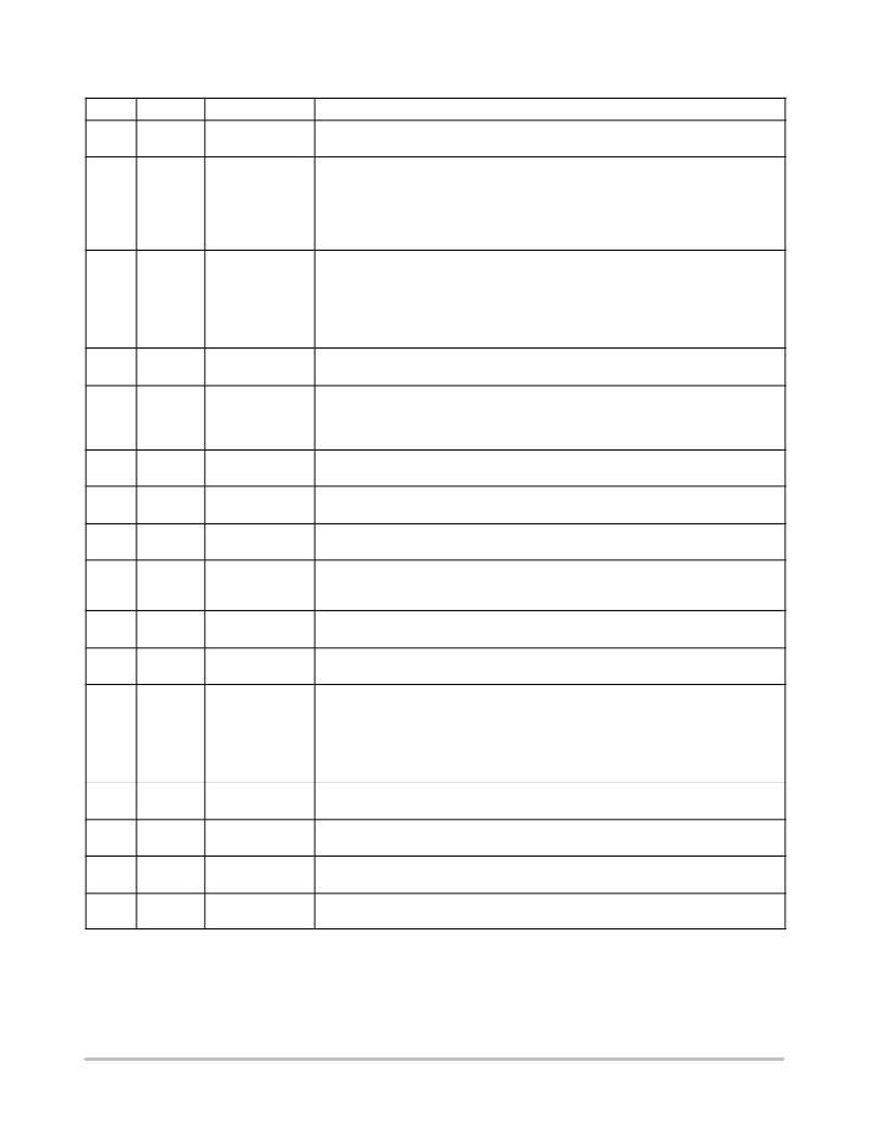 �
�
�NCP5604A,� NCP5604B�
�PIN� FUNCTION� DESCRIPTION�
�Pin�
�1�
�Symbol�
�VBAT�
�Type�
�INPUT,� POWER�
�Description�
�Input� Battery� voltage� to� supply� the� analog� and� digital� blocks.� The� pin� must� be� decoupled� to�
�ground� by� a� 1.0� m� F� ceramic� capacitor.�
�2�
�EN�
�INPUT,� DIGITAL�
�This� pin� carries� the� Enable� function� to� control� the� DC-DC� converter.� It� can� be� used� to�
�digitally� dim� the� LED� by� using� a� PWM� technique.�
�EN� =� Low� 3� shutdown� mode,� the� DC-DC� is� disconnected� from� the� load.�
�EN� =� High� 3� operating� mode,� the� DC-DC� is� activated.�
�The� digital� PWM� dimming� can� operate� over� the� 100� Hz� -� 200� kHz� frequency,� depending�
�upon� the� application� requirements.�
�3�
�I� REF�
�INPUT,� ANALOG�
�This� pin� provides� the� reference� current,� based� on� the� internal� bandgap� voltage� reference,�
�to� control� the� output� current� flowing� in� the� LED.� A� 1%� tolerance,� or� better,� resistor� shall� be�
�used� to� get� the� highest� accuracy� of� the� LED� biases.� An� external� current� source� can� be�
�used� to� bias� this� pin� to� dim� the� light� coming� out� of� the� LED.�
�In� no� case� shall� the� voltage� at� pin� 3� be� forced� either� higher� or� lower� than� the� 600� mV�
�provided� by� the� internal� reference.�
�4�
�AGND�
�POWER�
�This� pin� is� the� GROUND� signal� for� the� analog� and� digital� blocks� and� must� be� connected� to�
�the� system� ground.�
�5�
�LED4�
�INPUT,� POWER�
�NCP5604A:� This� pin� sinks� to� ground� and� monitors� the� current� flowing� into� the� fourth� LED,�
�intended� to� be� used� in� backlight� application.� The� current� is� limited� to� 25� mA� maximum�
�(Note� 2).�
�NCP5604B:� This� pin� is� not� connected.�
�6�
�LED3�
�INPUT,� POWER�
�This� pin� sinks� to� ground� and� monitors� the� current� flowing� into� the� third� LED,� intended� to� be�
�used� in� backlight� application.� The� current� is� limited� to� 25� mA� maximum� (Note� 2).�
�7�
�LED2�
�INPUT,� POWER�
�This� pin� sinks� to� ground� and� monitors� the� current� flowing� into� the� second� LED,� intended� to�
�be� used� in� backlight� application.� The� current� is� limited� to� 25mA� maximum� (Note� 2).�
�8�
�LED1�
�INPUT,� POWER�
�This� pin� sinks� to� ground� and� monitors� the� current� flowing� into� the� first� LED,� intended� to� be�
�used� in� backlight� application.� The� current� is� limited� to� 25� mA� maximum� (Note� 2).�
�9�
�PGND�
�POWER�
�This� pin� is� the� GROUND� reference� for� the� DC-DC� converter� and� the� output� current�
�control.� The� pin� must� be� connected� to� the� system� ground,� a� ground� plane� being� strongly�
�recommended.�
�10�
�C1N�
�POWER�
�One� side� of� the� external� charge� pump� capacitor� (C� FLY� )� is� connected� to� this� pin,� associated�
�with� C1P,� pin� 11� (Note� 1).�
�11�
�C1P�
�POWER�
�One� side� of� the� external� charge� pump� capacitor� (C� FLY� )� is� connected� to� this� pin,� associated�
�with� C1N,� pin� 10� (Note� 1).�
�12�
�VOUT�
�OUTPUT,� POWER�
�This� pin� provides� the� output� voltage� supplied� by� the� DC-DC� converter.� The� Vout� pin� must�
�be� bypassed� by� 1.0� m� F� ceramic� capacitor� located� as� close� as� possible� to� the� pin� to�
�properly� bypass� the� output� voltage� to� ground.� The� circuit� shall� not� operate� without� such�
�bypass� capacitor� properly� connected� to� the� Vout� pin.�
�The� output� voltage� is� internally� clamped� to� 5.5� V� in� the� event� of� no� load� situation.� On� the�
�other� hand,� the� output� current� is� limited� to� 100� mA� in� the� event� of� a� short� circuit� to� ground.�
�13�
�C2P�
�POWER�
�One� side� of� the� external� charge� pump� capacitor� (C� FLY� )� is� connected� to� this� pin,� associated�
�with� C2N,� pin� 14� (Note� 1).�
�14�
�C2N�
�POWER�
�One� side� of� the� external� charge� pump� capacitor� (C� FLY� )� is� connected� to� this� pin,� associated�
�with� C2P,� pin� 13� (Note� 1).�
�15�
�C3P�
�POWER�
�One� side� of� the� external� charge� pump� capacitor� (C� FLY� )� is� connected� to� this� pin,� associated�
�with� C3N,� pin� 16� (Note� 1).�
�16�
�C3N�
�POWER�
�One� side� of� the� external� charge� pump� capacitor� (C� FLY� )� is� connected� to� this� pin,� associated�
�with� C3P,� pin� 15� (Note� 1).�
�1.� Using� low� ESR� 1.0� m� F� ceramic� capacitor� is� mandatory� to� optimize� the� Charge� Pump� efficiency.� The� DC� Bias� effect� must� be� taken� into� account�
�when� selecting� the� ceramic� capacitor.� Smallest� foot� print� packages� (size� 0602� and� lower)� are� prone� to� strong� DC� bias� effect,� reducing� the� real�
�capacitance� significantly.�
�2.� Total� DC-DC� output� current� is� limited� to� 100� mA.�
�3.� The� exposed� flag� shall� be� connected� to� ground.�
�http://onsemi.com�
�5�
�相关PDF资料 |
PDF描述 |
|---|---|
| GSC05DRXH-S734 | CONN EDGECARD 10POS DIP .100 SLD |
| LQW18ANR12J00D | INDUCTOR 120NH 180MA 0603 |
| AGM31DRST-S288 | CONN EDGECARD EXTEND 62POS .156 |
| RN-0915S/HP | CONV DC/DC 1.25W 09VIN 15VOUT |
| ESA50DRMT-S273 | CONN EDGECARD 100POS .125 WW |
相关代理商/技术参数 |
参数描述 |
|---|---|
| NCP5604B | 制造商:ONSEMI 制造商全称:ON Semiconductor 功能描述:High Efficiency White LED Driver |
| NCP5604BMTR2G | 功能描述:LED照明驱动器 ANA LED DRIVER RoHS:否 制造商:STMicroelectronics 输入电压:11.5 V to 23 V 工作频率: 最大电源电流:1.7 mA 输出电流: 最大工作温度: 安装风格:SMD/SMT 封装 / 箱体:SO-16N |
| NCP5604D WAF | 制造商:ON Semiconductor 功能描述: |
| NCP5608 | 制造商:ONSEMI 制造商全称:ON Semiconductor 功能描述:Multiple LED Charge Pump Driver |
| NCP5608 AP93B WAF | 制造商:ON Semiconductor 功能描述: |
发布紧急采购,3分钟左右您将得到回复。