- 您现在的位置:买卖IC网 > PDF目录20648 > NCP5604BMTR2G (ON Semiconductor)IC DRIVER LED WHITE HE 16-WQFN PDF资料下载
参数资料
| 型号: | NCP5604BMTR2G |
| 厂商: | ON Semiconductor |
| 文件页数: | 8/15页 |
| 文件大小: | 0K |
| 描述: | IC DRIVER LED WHITE HE 16-WQFN |
| 产品变化通告: | Product Obsolescence 30/Jun/2011 |
| 标准包装: | 1 |
| 拓扑: | PWM,切换式电容器(充电泵) |
| 输出数: | 4 |
| 内部驱动器: | 是 |
| 类型 - 主要: | 背光,闪灯/白光 |
| 类型 - 次要: | 白色 LED |
| 频率: | 850kHz ~ 1.15MHz |
| 电源电压: | 2.7 V ~ 5.5 V |
| 输出电压: | 4.8 V ~ 6 V |
| 安装类型: | 表面贴装 |
| 封装/外壳: | 16-WFQFN 裸露焊盘 |
| 供应商设备封装: | 16-QFN(3x3) |
| 包装: | 剪切带 (CT) |
| 工作温度: | -40°C ~ 85°C |
| 其它名称: | NCP5604BMTR2GOSCT |
�� �
�
�NCP5604A,� NCP5604B�
�ANALOG� SECTION� (Typical� values� are� referenced� to� T� A� =� +25� °� C,� Min� &� Max� values� are� referenced� -40� °� C� to� +85� °� C� ambient�
�temperature,� operating� conditions� 2.85� V� <� Vbat� <� 5.5� V,� unless� otherwise� noted.)�
�Pin�
�3�
�3�
�-�
�Symbol�
�I� REF�
�V� REF�
�I� LEDR�
�Rating�
�Reference� Current� @� Vref� =� 600� mV� (Note� 11)�
�Reference� Voltage� (Note� 12)�
�Reference� Current� (IREF)� to� Output� LED� Current� Ratio�
�Min�
�1.0�
�-2%�
�-�
�Typ�
�-�
�600�
�260�
�Max�
�100�
�+2%�
�-�
�Unit�
�m� A�
�mV�
�-�
�11.� The� overall� output� current� tolerance� depends� upon� the� accuracy� of� the� external� resistor.� Using� 1%� or� better� resistor� is� recommended.�
�12.� The� external� circuit� must� not� force� the� I� REF� pin� voltage� either� higher� or� lower� than� the� 600� mV� specified.�
�DIGITAL� PARAMETERS� SECTION� (Typical� values� are� referenced� to� T� A� =� +25� °� C,� Min� &� Max� values� are� referenced� -40� °� C� to� +85� °� C�
�ambient� temperature,� operating� conditions� 2.85� V� <� Vbat� <� 5.5� V,� unless� otherwise� noted.)� Note:� Digital� inputs� undershoot� <� -� 0.30� V� to�
�ground,� Digital� inputs� overshoot� <� 0.30� V� to� V� BAT� .�
�Pin�
�2�
�2�
�2�
�Symbol�
�F� PWM�
�V� IH�
�V� IL�
�Rating�
�Input� Enable� PWM�
�Positive� Going� Input� High� Voltage� Threshold,� EN� Signal�
�Negative� Going� Input� High� Voltage� Threshold,� EN� Signal�
�Min�
�0.1�
�1.3�
�0�
�Typ�
�-�
�-�
�-�
�Max�
�200�
�V� BAT�
�0.4�
�Unit�
�kHz�
�V�
�V�
�APPLICATIONS� INFORMATION�
�DC-DC� OPERATION�
�The� converter� is� based� on� a� charge� pump� technique� to�
�generate� a� DC� voltage� capable� to� supply� the� White� LED�
�load� The� system� regulates� the� current� flowing� into� each�
�LED� by� means� of� internal� current� mirrors� associated� with�
�the� white� diodes.� Consequently,� the� output� voltage� will� be�
�voltage� is� based� on� a� temperature� compensated� Band� Gap�
�structure,� a� tight� tolerance� resistor� will� provide� a� very�
�accurate� load� current.� The� resistor� is� calculated� from� the�
�Ohm's� law� (R� bias� =� Vref/I� REF� )� and� a� more� practical�
�equation� can� be� arranged� to� define� the� resistor� value� for� a�
�given� output� current:�
�equal� to� the� Vf� of� the� LED,� plus� the� 300� mV� (typical)�
�developed� across� the� internal� NMOS� mirror.� Typically,�
�assuming� a� standard� white� LED� forward� biased� at� 10� mA,�
�the� output� voltage� will� be� 3.8� V.�
�Rbias� +� (Vref� *� k)� Iout�
�Rbias� +� (0.6� *� 260)� Iout�
�Rbias� +� 156� Iout�
�(eq.� 1)�
�(eq.� 2)�
�The� third� external� capacitor� makes� possible� the� 1.33X�
�extra� mode� of� operation,� with� a� significant� efficiency�
�improvement� of� the� converter� over� the� normal� battery�
�voltage� span.� The� threshold� levels� have� been� defined� to�
�optimize� this� range� of� operating� voltage,� assuming� a� high�
�efficiency� is� not� relevant� when� the� system� is� connected� to�
�a� battery� charger� (� i.e.� Vbat� >� 4.5� V).�
�The� built-in� OVP� circuit� continuously� monitor� each�
�output� and� stops� the� converter� when� the� voltage� is� above�
�5.0� V.� The� converter� resumes� to� normal� operation� when� the�
�voltage� drops� below� 5.0� V� (no� latch-up� mechanism).�
�Consequently,� the� chip� can� operate� with� no� load� during� any�
�test� procedures,� but� in� the� case� of� special� applications,� it� is�
�Consequently,� the� resistor� value� will� range� between�
�R� bias� =� 156/25� mA� =� 6240� W� and� R� bias� =� 156/0.5� mA� =�
�312� k� W� .� Obviously,� the� tolerance� of� such� a� resistor� must� be�
�1%� or� better,� with� a� 100� ppm� thermal� coefficient,� to� get� the�
�expected� overall� tolerance.�
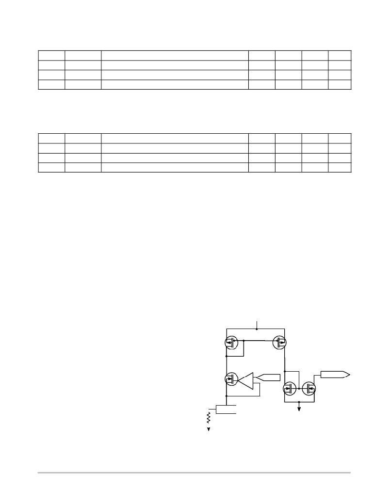
�VBandGap�
�LED� Return�
�recommended� to� connect� the� non� used� LED� driver� either� to�
�a� LED,� or� to� the� Vbat� supply� to� minimize� the� internal� losses�
�(see� LOAD� CONNECTION� paragraph).�
�+�
�-�
�600mV�
�Pin� 5� to� 8�
�LOAD� CURRENT� CALCULATION�
�The� load� current� is� derived� from� the� 600� mV� reference�
�voltage� provided� by� the� internal� Band� Gap� associated� to� the�
�I� REF�
�Pin� 3�
�GND�
�external� resistor� connected� across� I� REF� pin� and� Ground� (see�
�Figure� 4).� In� any� case,� no� voltage� shall� be� forced� at� I� REF�
�pin,� either� downward� or� upward.�
�The� reference� current� is� multiplied� by� the� constant�
�GND�
�Note:� The� I� REF� pin� must� never� be� biased�
�to� voltage� higher� than� 600� mV.�
�Figure� 4.� Basic� Reference� Current� Source�
�k� =� 260� to� yield� the� output� load� current.� Since� the� reference�
�http://onsemi.com�
�8�
�相关PDF资料 |
PDF描述 |
|---|---|
| S2K-13 | RECTIFIER GPP SMD 800V 1.5A SMB |
| VE-BNV-EV-B1 | CONVERTER MOD DC/DC 5.8V 150W |
| VE-BNV-EU-F3 | CONVERTER MOD DC/DC 5.8V 200W |
| ISL89412IPZ | IC DVR MOSFET DUAL-CH 8-PDIP |
| VE-J6V-CX-F2 | CONVERTER MOD DC/DC 5.8V 75W |
相关代理商/技术参数 |
参数描述 |
|---|---|
| NCP5604D WAF | 制造商:ON Semiconductor 功能描述: |
| NCP5608 | 制造商:ONSEMI 制造商全称:ON Semiconductor 功能描述:Multiple LED Charge Pump Driver |
| NCP5608 AP93B WAF | 制造商:ON Semiconductor 功能描述: |
| NCP5608EVB | 功能描述:电源管理IC开发工具 NCP5608 EVAL BRD RoHS:否 制造商:Maxim Integrated 产品:Evaluation Kits 类型:Battery Management 工具用于评估:MAX17710GB 输入电压: 输出电压:1.8 V |
| NCP5608MTR2G | 功能描述:LED照明驱动器 MULT LED BOOST DR RoHS:否 制造商:STMicroelectronics 输入电压:11.5 V to 23 V 工作频率: 最大电源电流:1.7 mA 输出电流: 最大工作温度: 安装风格:SMD/SMT 封装 / 箱体:SO-16N |
发布紧急采购,3分钟左右您将得到回复。