- 您现在的位置:买卖IC网 > Datasheet目录996 > NCP5608EVB (ON Semiconductor)EVAL BOARD FOR NCP5608 Datasheet资料下载
参数资料
| 型号: | NCP5608EVB |
| 厂商: | ON Semiconductor |
| 文件页数: | 4/16页 |
| 文件大小: | 0K |
| 描述: | EVAL BOARD FOR NCP5608 |
| 设计资源: | NCP5608EVB BOM NCP5608EVB Gerber Files NCP5608EVB Schematic NCP5608 Demo Brd BOM |
| 标准包装: | 1 |
| 电流 - 输出 / 通道: | 500mA |
| 输出及类型: | 8,非隔离 |
| 输出电压: | 4.8 ~ 5.5 V |
| 特点: | 亮度控制 |
| 输入电压: | 3.6V |
| 已供物品: | 板 |
| 已用 IC / 零件: | NCP5608 |
| 其它名称: | NCP5608EVBOS |
��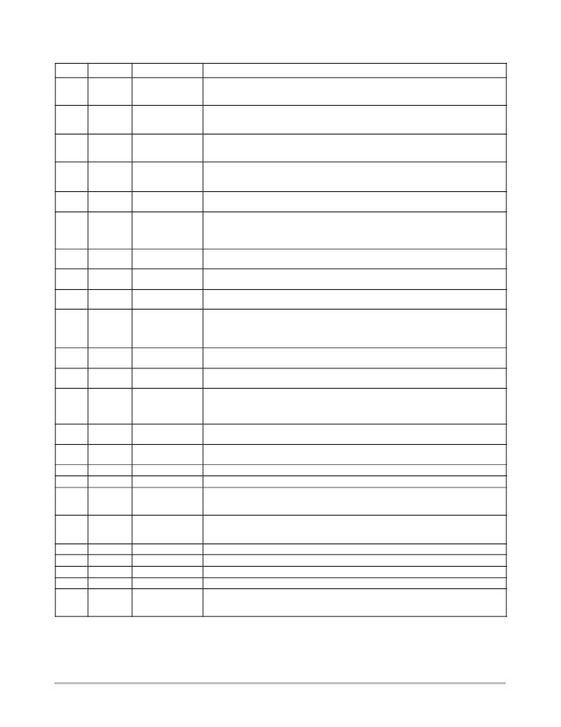 �
�
�NCP5608�
�PIN� FUNCTION� DESCRIPTION�
�Pin�
�1�
�Symbol�
�AGND�
�Type�
�GROUND�
�Description�
�This� pin� is� the� NCP5608� analog� ground� and� shall� be� connected� to� the� system� ground.� Care�
�must� be� observed� to� minimize� the� total� parasitic� inductance� between� the� pin� and� the� ground�
�plane.�
�2�
�IREFFL�
�OUTPUT,� ANALOG�
�This� pin� is� used� to� set� up� the� current� reference� for� the� FLASH� output� currents� (LED5� to�
�LED8).� The� reference� current� is� derived� from� the� internal� bandgap� voltage� to� ground� by�
�means� of� an� external� resistor.� (Note� 1)�
�3�
�IREFBK�
�OUTPUT,� ANALOG�
�This� pin� is� used� to� set� up� the� current� reference� for� the� BACK� LIGHT� output� currents� (LED1�
�to� LED4).� The� reference� current� is� derived� from� the� internal� bandgap� voltage� to� ground� by�
�means� of� an� external� resistor.� (Note� 1)�
�4�
�SDA�
�INPUT,� DIGITAL�
�This� pin,� associated� with� the� SCL� signal,� carries� the� DATA� signal� to� set� up� the� selected�
�output� LED� current.�
�The� DATA� signal� is� built� with� a� single� SDA� line� to� support� the� I2C� protocol.�
�5�
�SCL�
�INPUT,� DIGITAL�
�This� is� the� clock� signal� associated� with� the� SDA� pins.� The� pin� carries� the� standard� CLOCK�
�signal� to� operate� the� I2C� protocol.�
�6�
�CCMP�
�ANALOG,� INPUT�
�This� pin� is� connected� to� the� internal� I2C� bias� network� and� must� be� either� left� open,� or�
�bypassed� to� ground� by� a� 10� nF� ceramic� capacitor� when� the� I2C� voltage� drops� below� 1.8� V.�
�Such� a� capacitor� compensate� the� voltage� drop� during� normal� operation,� keeping� in� mind� it� is�
�not� mandatory� when� the� I2C� voltage� is� 1.8� V� and� above.�
�7�
�LED1�
�INPUT,� POWER�
�This� pin� sinks� to� ground� the� current� flowing� into� the� first� LED,� and� is� intended� to� be� used� in�
�backlight� application.� The� current� is� limited� to� 30� mA� max.� (Note� 2)�
�8�
�LED2�
�INPUT,� POWER�
�This� pin� sinks� to� ground� the� current� flowing� into� the� second� LED,� and� is� intended� to� be� used�
�in� backlight� application.� The� current� is� limited� to� 30� mA� max.� (Note� 2)�
�9�
�LED3�
�INPUT,� POWER�
�This� pin� sinks� to� ground� the� current� flowing� into� the� third� LED,� and� is� intended� to� be� used� in�
�backlight� application.� The� current� is� limited� to� 30� mA� max.� (Note� 2)�
�10�
�LED4�
�INPUT,� POWER�
�This� pin� sinks� to� ground� the� current� flowing� into� the� fourth� LED,� and� is� intended� to� be� used�
�in� backlight� application.� The� current� is� limited� to� 30� mA� max.� (Note� 2)�
�On� the� other� hand,� LED4� can� be� disconnected� when� only� three� LEDs� are� used� in� the�
�backlight� application.� (Table� 1)�
�11�
�LED5�
�INPUT,� POWER�
�This� pin� sinks� to� ground� the� current� flowing� into� the� fifth� LED� (100� mA� max),� and� is� intended�
�to� be� used� in� Flash� application.� (Note� 2)�
�12�
�LED6�
�INPUT,� POWER�
�This� pin� sinks� to� ground� the� current� flowing� into� the� sixth� LED� (100� mA� max),� and� is�
�intended� to� be� used� in� Flash� or� high� power� application.� (Note� 2)�
�13�
�PWRGND�
�POWER�
�This� pin� provides� the� ground� reference� for� the� power� elements� and� must� be� connected� to�
�the� system� ground� by� a� heavy� track.� Using� the� ground� plane� technique� is� strongly�
�recommended.� Care� must� be� observed� to� minimize� the� total� parasitic� inductance� between�
�the� pin� and� the� ground� plane.�
�14�
�LED7�
�INPUT,� POWER�
�This� pin� sinks� to� ground� the� current� flowing� into� the� seventh� LED� (100� mA� max),� and� is�
�intended� to� be� used� in� flash� or� high� power� application.� (Note� 2)�
�15�
�LED8�
�INPUT,� POWER�
�This� pin� sinks� to� ground� the� current� flowing� into� the� eighth� LED� (100� mA� max),� and� is�
�intended� to� be� used� in� flash� or� high� power� application.� (Note� 2)�
�16�
�17�
�18�
�C1N�
�C1P�
�VOUT�
�POWER�
�POWER�
�OUTPUT,� POWER�
�This� pin� is� the� second� side� of� the� C1� fly� capacitor.�
�This� pin� is� the� first� side� of� the� C1� fly� capacitor.�
�This� pin� provides� the� output� power� to� the� external� LED.� Since� the� regulation� is� based� on� a�
�current� loop,� the� voltage� will� varies� as� the� output� current� varies� in� the� application.� The� Vout�
�pin� must� be� bypassed� to� GND� by� a� 4.7� m� F� ceramic� capacitor.� (Note� 3)�
�19�
�PVBAT�
�INPUT,� POWER�
�This� pin� provides� the� supply� voltage� to� the� charge� pump� converter.� The� pin� must� be�
�connected� to� the� AVbat� supply� source� and� bypassed� to� GND� by� a� 10� m� F/16� V� ceramic�
�capacitor.� (Note� 3)� Using� a� power� plane� is� recommended.�
�20�
�21�
�22�
�23�
�24�
�C2N�
�C2P�
�C3P�
�C3N�
�AVbat�
�POWER�
�POWER�
�POWER�
�POWER�
�INPUT,� POWER�
�This� pin� is� the� second� side� of� the� C2� fly� capacitor.�
�This� pin� is� the� first� side� of� the� C2� fly� capacitor.�
�This� pin� is� the� second� side� of� the� C3� fly� capacitor.�
�This� pin� is� the� first� side� of� the� C3� fly� capacitor.�
�This� pin� provides� the� supply� voltage� to� the� analog� and� digitals� blocks.� The� pin� must� be�
�connected� to� the� PVbat� supply� source� and� bypassed� to� GND� by� a� 1� m� F/16� V� ceramic�
�capacitor.� (Note� 3)� Using� a� power� plane� is� recommended.�
�1.� To� achieve� a� good� accuracy� of� the� LED� current,� 1%� tolerance� resistor,� with� 100� ppm� stability,� or� better,� shall� be� used.� The� reference� current�
�is� internally� mirrored� and� sized� according� to� the� programmed� value� for� a� given� external� LED.�
�2.� Total� DC?DC� output� current� is� limited� to� 500� mA.�
�3.� Ceramic� X7R,� ESR� <� 50� m� W� ESL� <� 0.5� nH,� SMD� types� capacitors� are� mandatory� to� achieve� the� Iout� specifications.� On� the� other� hand,� care�
�must� be� observed� to� take� into� account� the� DC� bias� impact� on� the� capacitance� value;� see� ceramic� capacitor� manufacturer� data� sheets.�
�http://onsemi.com�
�4�
�相关PDF资料 |
PDF描述 |
|---|---|
| NCP5612GEVB | EVAL BOARD FOR NCP5612G |
| NCV7680PWR22GEVB | BOARD EVALUATION NCV7680 |
| NDNA200 | DIN-RAIL 35MM ALUMINUM 2M |
| NG-9517 | CABLE GLAND NEMA 4X PG-29 BLACK |
| NH2503K000FJ01 | 250WATTS 3KOHMS 1% NON-INDUCTIVE |
相关代理商/技术参数 |
参数描述 |
|---|---|
| NCP5608MTR2G | 功能描述:LED照明驱动器 MULT LED BOOST DR RoHS:否 制造商:STMicroelectronics 输入电压:11.5 V to 23 V 工作频率: 最大电源电流:1.7 mA 输出电流: 最大工作温度: 安装风格:SMD/SMT 封装 / 箱体:SO-16N |
| NCP561 | 制造商:ONSEMI 制造商全称:ON Semiconductor 功能描述:AC-DC Offline Switching Controllers/Regulators |
| NCP561/D | 制造商:未知厂家 制造商全称:未知厂家 功能描述:150 mA CMOS Low Iq Low-Dropout Voltage Regulator |
| NCP5612 | 制造商:ONSEMI 制造商全称:ON Semiconductor 功能描述:High Efficiency Ultra Small Thinnest White LED Driver |
| NCP5612GEVB | 功能描述:LED 照明开发工具 NCP5612 EVAL BRD RoHS:否 制造商:Fairchild Semiconductor 产品:Evaluation Kits 用于:FL7732 核心: 电源电压:120V 系列: 封装: |
发布紧急采购,3分钟左右您将得到回复。