- 您现在的位置:买卖IC网 > PDF目录22018 > NCP580SQ33T1G (ON Semiconductor)IC REG LDO 3.3V .12A SC82AB PDF资料下载
参数资料
| 型号: | NCP580SQ33T1G |
| 厂商: | ON Semiconductor |
| 文件页数: | 2/9页 |
| 文件大小: | 0K |
| 描述: | IC REG LDO 3.3V .12A SC82AB |
| 产品变化通告: | Product Discontinuation 09/Jan/2008 |
| 标准包装: | 1 |
| 稳压器拓扑结构: | 正,固定式 |
| 输出电压: | 3.3V |
| 输入电压: | 最高 6V |
| 电压 - 压降(标准): | 0.18V @ 120mA |
| 稳压器数量: | 1 |
| 电流 - 输出: | 120mA(最小) |
| 工作温度: | -40°C ~ 85°C |
| 安装类型: | 表面贴装 |
| 封装/外壳: | SC-82A,SOT-343 |
| 供应商设备封装: | SC-82AB |
| 包装: | 剪切带 (CT) |
| 其它名称: | NCP580SQ33T1GOSCT NCP580SQ33T1OSCT NCP580SQ33T1OSCT-ND |
�� �
�
�NCP580�
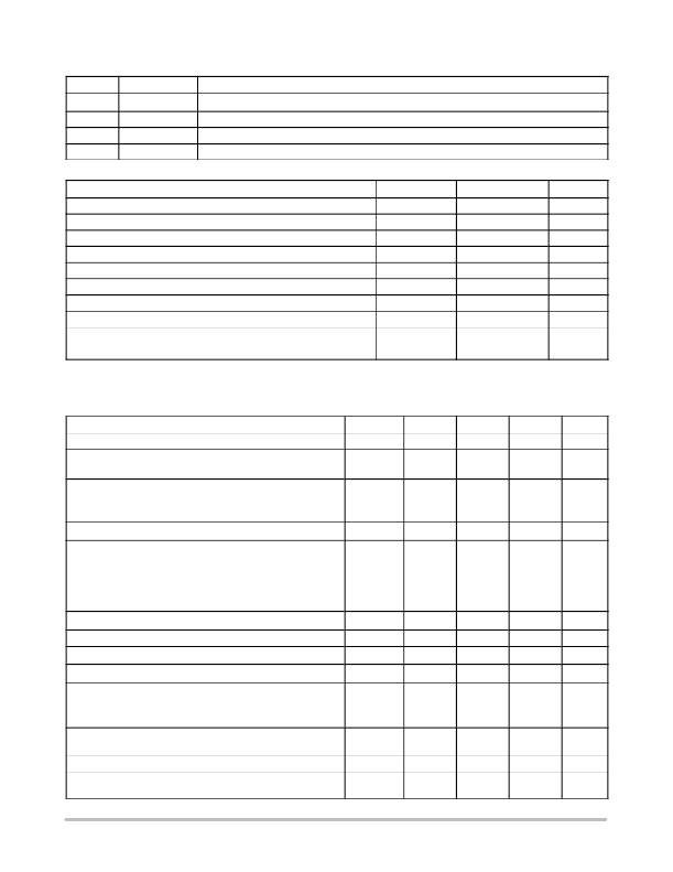
�PIN� FUNCTION� DESCRIPTION�
�Pin�
�1�
�2�
�3�
�4�
�Symbol�
�Vout�
�GND�
�CE�
�V� in�
�Regulated� output� voltage.�
�Power� supply� ground.�
�Chip� enable� pin.�
�Power� supply� input� voltage.�
�Description�
�MAXIMUM� RATINGS�
�Rating�
�Input� Voltage�
�Input� Voltage� (CE� Pin)�
�Output� Voltage�
�Output� Current�
�Power� Dissipation�
�ESD� Capability,� Human� Body� Model,� C� =� 100� pF,� R� =� 1.5� k� W�
�ESD� Capability,� Machine� Model,� C� =� 200� pF,� R� =� 0� W�
�Operating� Ambient� Temperature� Range�
�Maximum� Junction� Temperature�
�Storage� Temperature� Range�
�Symbol�
�V� in�
�V� CE�
�V� out�
�I� out�
�P� D�
�ESD� HBM�
�ESD� MM�
�T� A�
�T� J(max)�
�T� stg�
�Value�
�6.5�
�-0.3� to� V� in� +0.3�
�-0.3� to� V� in� +0.3�
�140�
�150�
�1500�
�150�
�-40� to� +85�
�125�
�-55� to� +150�
�Unit�
�V�
�V�
�V�
�mA�
�mW�
�V�
�V�
�°� C�
�°� C�
�°� C�
�Stresses� exceeding� Maximum� Ratings� may� damage� the� device.� Maximum� Ratings� are� stress� ratings� only.� Functional� operation� above� the�
�Recommended� Operating� Conditions� is� not� implied.� Extended� exposure� to� stresses� above� the� Recommended� Operating� Conditions� may� affect�
�device� reliability.�
�ELECTRICAL CHARACTERISTICS� (V� in� = V� out� + 1.0 V, T� A� = 25� °� C� ,� unless� otherwise� noted.)�
�Characteristic�
�Input� Voltage�
�Output� Voltage� (I� out� =� 1.0� mA� to� 30� mA)�
�Line� Regulation� (I� out� =� 30� mA)�
�Symbol�
�V� in�
�V� out�
�Reg� line�
�Min�
�2.2�
�V� out� X�
�0.985�
�-�
�Typ�
�-�
�-�
�0.02�
�Max�
�6.0�
�V� out� X�
�1.015�
�0.10�
�Unit�
�V�
�V�
�%/V�
�(V� out� +� 0.5� V� v� V� in� v� 6.0� V)�
�(V� out� =� 1.5� V,� 2.2� V� v� V� in� v� 6.0� V)�
�Load� Regulation� (I� out� =� 1.0� mA� to� 120� mA)�
�Reg� load�
�-�
�12�
�40�
�mV�
�Dropout� Voltage� (I� out� =� 120� mA)�
�V� DO�
�V�
�V� out� =� 1.5� V�
�V� out� =� 1.8� V�
�V� out� =� 2.5� V�
�2.8� V� v� V� out� v� 3.3� V�
�-�
�-�
�-�
�-�
�0.36�
�0.28�
�0.24�
�0.18�
�0.70�
�0.40�
�0.35�
�0.28�
�Quiescent� Current� (I� out� =� 0� mA)�
�Output� Current�
�Shutdown� Current� (V� in� =� V� CE� )�
�Output� Short� Circuit� Current� (V� out� =� 0)�
�Ripple� Rejection� (I� out� =� 30� mA)� f� =� 1.0� kHz�
�(V� out� =� 1.5� V,� V� in� –� V� out� =� 1.2� V)�
�(V� out� w� 2.5� V,� V� in� –� V� out� =� 1.0� V)�
�Enable� Input� Threshold� Voltage� -� High�
�Enable� Input� Threshold� Voltage� -� Low�
�Output� Noise� Voltage� (Bandwidth� =� 10� Hz� to� 100� kHz)�
�Output� Voltage� Temperature� Coefficient�
�(I� out� =� 30� mA,� -40� °� C� v� T� A� v� 85� °� C)�
�Iq�
�I� out�
�I� SD�
�I� lim�
�RR�
�Vth� enh�
�Vth� enl�
�V� n�
�D� V� out� /� D� T�
�-�
�120�
�-�
�-�
�-�
�1.5�
�0�
�-�
�-�
�90�
�-�
�0.1�
�40�
�75�
�70�
�-�
�-�
�30�
�"� 100�
�160�
�-�
�1.0�
�-�
�-�
�-�
�V� in�
�0.3�
�-�
�-�
�m� A�
�mA�
�m� A�
�mA�
�dB�
�V�
�m� Vrms�
�ppm/� °� C�
�http://onsemi.com�
�2�
�相关PDF资料 |
PDF描述 |
|---|---|
| EP4CE15F17C7N | IC CYCLONE IV E FPGA 15K 256FBGA |
| ACM02DRTN | CONN EDGECARD 4POS DIP .156 SLD |
| EPF10K10LC84-4 | IC FLEX 10K FPGA 84-PLCC |
| ESC65DRES-S734 | CONN EDGECARD 130POS .100 EYELET |
| EPF10K10LC84-4N | IC FLEX 10K FPGA 84-PLCC |
相关代理商/技术参数 |
参数描述 |
|---|---|
| NCP5810AX66B WAF | 制造商:ON Semiconductor 功能描述: |
| NCP5810CMUTXG | 功能描述:LED照明驱动器 DUAL AMOLED DRV SPLY RoHS:否 制造商:STMicroelectronics 输入电压:11.5 V to 23 V 工作频率: 最大电源电流:1.7 mA 输出电流: 最大工作温度: 安装风格:SMD/SMT 封装 / 箱体:SO-16N |
| NCP5810CUMUTXG | 功能描述:LED显示驱动器 DUAL AMOLED DRV SPLY RoHS:否 制造商:Micrel 数位数量:5 片段数量: 安装风格:SMD/SMT 封装 / 箱体:PLCC-44 工作电源电压:4.75 V to 11 V 最大电源电流:10 mA 最大工作温度:+ 85 C 最小工作温度:- 40 C 封装:Tube |
| NCP5810D AP10C WAF | 制造商:ON Semiconductor 功能描述: |
| NCP5810D AP10D WAF | 制造商:ON Semiconductor 功能描述: |
发布紧急采购,3分钟左右您将得到回复。