- 您现在的位置:买卖IC网 > PDF目录19208 > NCP700MN180R2G (ON Semiconductor)IC REG LDO 1.8V .2A 6-DFN PDF资料下载
参数资料
| 型号: | NCP700MN180R2G |
| 厂商: | ON Semiconductor |
| 文件页数: | 8/10页 |
| 文件大小: | 0K |
| 描述: | IC REG LDO 1.8V .2A 6-DFN |
| 产品变化通告: | NCV8570, NCP700/3985 Discontinuation 20/Aug/2011 |
| 标准包装: | 1 |
| 稳压器拓扑结构: | 正,固定式 |
| 输出电压: | 1.8V |
| 输入电压: | 2.5 V ~ 5.5 V |
| 稳压器数量: | 1 |
| 电流 - 输出: | 200mA |
| 电流 - 限制(最小): | 200mA |
| 工作温度: | -40°C ~ 85°C |
| 安装类型: | 表面贴装 |
| 封装/外壳: | 6-VDFN 裸露焊盘 |
| 供应商设备封装: | 6-DFN(2x2.2) |
| 包装: | 标准包装 |
| 产品目录页面: | 1120 (CN2011-ZH PDF) |
| 其它名称: | NCP700MN180R2GOSDKR |
�� �
�
�NCP700�
�APPLICATION� INFORMATION�
�P� D� +�
�General�
�The� NCP700� is� a� 200� mA� (current� limited)� linear�
�regulator� with� a� logic� input� for� on/off� control� for� the� high�
�speed� turn� ?� off� output� voltage.�
�Access� to� the� major� contributor� of� noise� within� the�
�integrated� circuit� is� provided� as� the� focus� for� noise� reduction�
�within� the� linear� regulator� system.�
�Power� Up/Down�
�During� power� up,� the� NCP700� maintains� a� high�
�impedance� output� (V� out� )� until� sufficient� voltage� is� present� on�
�V� in� to� power� the� internal� bandgap� reference� voltage.� When�
�sufficient� voltage� is� supplied� (approx� 1.2� V),� V� out� will� start�
�to� turn� on� (assume� CE� shorted� to� V� in� ),� linearly� increasing�
�until� the� output� regulation� voltage� has� been� reached.�
�Active� discharge� circuitry� has� been� implemented� to� insure�
�a� fast� turn� off� time.� Then� CE� goes� low,� the� active� discharge�
�transistor� turns� on� creating� a� fast� discharge� of� the� output�
�voltage.� Power� to� drive� this� circuitry� is� drawn� from� the�
�output� node.� This� is� to� maintain� the� lowest� quiescent� current�
�when� in� the� sleep� mode� (V� CE� =� 0.4� V).� This� circuitry�
�subsequently� turns� off� when� the� output� voltage� discharges.�
�CE� (chip� enable)�
�The� enable� function� is� controller� by� the� logic� pin� CE.� The�
�voltage� threshold� of� this� pin� is� set� between� 0.4� V� and� 1.2� V.�
�A� voltage� lower� than� 0.4� V� guarantees� the� device� is� off.� A�
�voltage� higher� than� 1.2� V� guarantees� the� device� is� on.� The�
�NCP700� enters� a� sleep� mode� when� in� the� off� state� drawing�
�less� than� 1� m� A� of� quiescent� current.�
�The� device� can� be� used� as� a� simple� regulator� without� use�
�of� the� chip� enable� feature� by� tying� the� CE� pin� to� the� V� in� pin.�
�Current� Limit�
�Output� Current� is� internally� limited� within� the� IC� to� a�
�Output� Noise�
�The� main� contributor� for� noise� present� on� the� output� pin�
�V� out� is� the� reference� voltage� node.� This� is� because� any� noise�
�which� is� generated� at� this� node� will� be� subsequently�
�amplified� through� the� error� amplifier� and� the� PMOS� pass�
�device.� Access� to� the� reference� voltage� node� is� supplied�
�directly� through� the� C� noise� pin.� Noise� can� be� reduced� from�
�a� typical� value� of� 20� m� V� rms� by� using� 10� nF� to� 15� m� V� rms� by�
�using� a� 100� nF� from� the� C� noise� pin� to� ground.�
�A� bypass� capacitor� is� recommended� for� good� noise�
�performance� and� better� load� transient� response.�
�Thermal� Shutdown�
�When� the� die� temperature� exceeds� the� Thermal� Shutdown�
�threshold,� a� Thermal� Shutdown� (TSD)� event� is� detected� and�
�the� output� (V� out� )� is� turned� off.� There� is� no� effect� from� the�
�active� discharge� circuitry.� The� IC� will� remain� in� this� state�
�until� the� die� temperature� moves� below� the� shutdown�
�threshold� (150� °� C� typical)� minus� the� hysteresis� factor� (20� °� C�
�typical).�
�This� feature� provides� protection� from� a� catastrophic�
�device� failure� due� to� accidental� overheating.� It� is� not�
�intended� to� be� used� as� a� substitute� for� proper� heat� sinking.�
�The� maximum� device� power� dissipation� can� be� calculated�
�by:�
�T� J� *� T� A�
�R� q� JA�
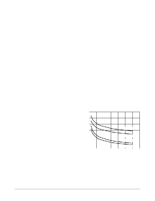
�Thermal� resistance� value� versus� copper� area� and� package� is�
�shown� in� Figure� 24.�
�380�
�330�
�minimum� of� 200� mA.� The� design� is� set� to� a� higher� value� to�
�allow� for� variation� in� processing� and� the� temperature�
�coefficient� of� the� parameter.� The� NCP700� will� source� this�
�amount� of� current� measured� with� a� voltage� 100� mV� lower�
�280�
�230�
�TSOP� ?� 5� (1� oz)�
�than� the� typical� operating� output� voltage.�
�The� specification� for� short� circuit� current� limit� (@� V� out� =�
�0� V)� is� specified� at� 320� mA� (typ).� There� is� no� additional�
�circuitry� to� lower� the� current� limit� at� low� output� voltages.�
�This� number� is� provided� for� informational� purposes� only.�
�Output� Capacitor�
�The� NCP700� has� been� designed� to� work� with� low� ESR�
�ceramic� capacitors.� There� is� no� ESR� lower� limit� for� stability�
�for� the� recommended� 1� m� F� output� capacitor.� Stable� region�
�for� Output� capacitor� ESR� vs� Output� Current� is� shown� in�
�180�
�130�
�80�
�0�
�TSOP� ?� 5� (2� oz)�
�DFN6 2x2.2 (1 oz)�
�DFN6 2x2.2 (2 oz)�
�100� 200� 300� 400� 500� 600� 700�
�PCB� COPPER� AREA� (mm� 2� )�
�Figure� 24.� R� q� JA� vs.� PCB� Copper� Area�
�(TSOP� ?� 5� for� comparison� only)�
�Figure� 23.�
�Typical� characteristics� were� measured� with� Murata�
�ceramic� capacitors.� GRM219R71E105K� (1� m� F,� 25� V,� X7R,�
�0805)� and� GRM21BR71A106K� (10� m� F,� 10� V,� X7R,� 0805).�
�http://onsemi.com�
�8�
�相关PDF资料 |
PDF描述 |
|---|---|
| VE-B50-CW-S | CONVERTER MOD DC/DC 5V 100W |
| RCC13DRYH-S13 | CONN EDGECARD 26POS .100 EXTEND |
| VE-B4X-CW-S | CONVERTER MOD DC/DC 5.2V 100W |
| MBRS320T3G | DIODE SCHOTTKY 20V 4A SMC |
| GBM10DRSN | CONN EDGECARD 20POS DIP .156 SLD |
相关代理商/技术参数 |
参数描述 |
|---|---|
| NCP700MN250R2G | 功能描述:低压差稳压器 - LDO RF LDO / 150mA RoHS:否 制造商:Texas Instruments 最大输入电压:36 V 输出电压:1.4 V to 20.5 V 回动电压(最大值):307 mV 输出电流:1 A 负载调节:0.3 % 输出端数量: 输出类型:Fixed 最大工作温度:+ 125 C 安装风格:SMD/SMT 封装 / 箱体:VQFN-20 |
| NCP700MN275R2G | 功能描述:低压差稳压器 - LDO RF LDO / 150mA RoHS:否 制造商:Texas Instruments 最大输入电压:36 V 输出电压:1.4 V to 20.5 V 回动电压(最大值):307 mV 输出电流:1 A 负载调节:0.3 % 输出端数量: 输出类型:Fixed 最大工作温度:+ 125 C 安装风格:SMD/SMT 封装 / 箱体:VQFN-20 |
| NCP700MN280R2G | 功能描述:低压差稳压器 - LDO LO NOISE HI PSSR BiCMOS RF LDO 150mA RoHS:否 制造商:Texas Instruments 最大输入电压:36 V 输出电压:1.4 V to 20.5 V 回动电压(最大值):307 mV 输出电流:1 A 负载调节:0.3 % 输出端数量: 输出类型:Fixed 最大工作温度:+ 125 C 安装风格:SMD/SMT 封装 / 箱体:VQFN-20 |
| NCP700MN300R2G | 功能描述:低压差稳压器 - LDO LO NOISE HI PSSR BiCMOS RF LDO 150mA RoHS:否 制造商:Texas Instruments 最大输入电压:36 V 输出电压:1.4 V to 20.5 V 回动电压(最大值):307 mV 输出电流:1 A 负载调节:0.3 % 输出端数量: 输出类型:Fixed 最大工作温度:+ 125 C 安装风格:SMD/SMT 封装 / 箱体:VQFN-20 |
| NCP700MN330R2G | 功能描述:低压差稳压器 - LDO RF LDO / 150mA RoHS:否 制造商:Texas Instruments 最大输入电压:36 V 输出电压:1.4 V to 20.5 V 回动电压(最大值):307 mV 输出电流:1 A 负载调节:0.3 % 输出端数量: 输出类型:Fixed 最大工作温度:+ 125 C 安装风格:SMD/SMT 封装 / 箱体:VQFN-20 |
发布紧急采购,3分钟左右您将得到回复。