- 您现在的位置:买卖IC网 > PDF目录16377 > NCS2563DGEVB (ON Semiconductor)BOARD EVALUATION NCS2563D PDF资料下载
参数资料
| 型号: | NCS2563DGEVB |
| 厂商: | ON Semiconductor |
| 文件页数: | 7/9页 |
| 文件大小: | 0K |
| 描述: | BOARD EVALUATION NCS2563D |
| 设计资源: | NCS2563 Schematic NCS2563 BOM |
| 标准包装: | 1 |
| 主要目的: | 视频,放大器,三路 |
| 嵌入式: | 否 |
| 已用 IC / 零件: | NCS2563 |
| 主要属性: | 增益 6dB,重构滤波器 |
| 次要属性: | AC 或 DC 耦合输入和输出 |
| 已供物品: | 板 |
| 其它名称: | NCS2563DGEVBOS |
NCS2563
http://onsemi.com
7
APPLICATIONS INFORMATION
The NCS2563 triple video driver has been optimized for
High Definition video applications covering the
requirements of the standards 720p, 1080i and related
(RGB). All the 3 channels feature the same specifications
and
similar
behaviors
guaranteed
by
a
high
channeltochannel crosstalk isolation (down to 60 dB at
1 MHz).
Each
channel
provides
an
internal
voltagetovoltage gain of 2 from its input to its output
reducing by the way the number of external components
usually needed in the case of some discrete approaches
(using standalone op amps). An internal level shifter is
employed shifting up the output voltage by adding an offset
of about 280 mV. This avoids sync pulse clipping and allows
DCcoupled output to the 150
W video load. In addition, the
NCS2563 integrates a 6th order Butterworth filter per
channel with a 3 dB frequency bandwidth of 30 MHz. This
allows rejecting out the aliases or unwanted oversampling
effects produced by the video DAC. It works the same way
for DVD recorders using ADC, this antialiasing filter
(reconstruction filter) will avoid picture quality issue and
will help also to filter out parasitic signals caused by EMI
interference.
A builtin diodelike clamp is used into the chip for each
channel to support ACcoupled mode of operation. The
clamp is active when the input signal goes below 0 V.
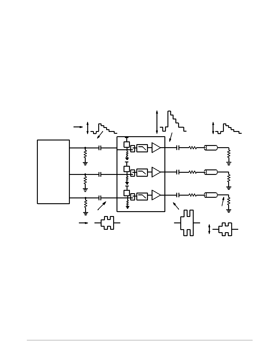
Figure 11. ACCoupled Inputs and Outputs
DAC
0V
1V
2.28V
0.28V
75W
1VPP
0.7VPP
ZO = 75W
75W
220mF
OUT1
OUT2
OUT3
2.28V
0.28V
0.1mF
RS
IN1
IN2
IN3
Y, R’, G’, B’
Pb, Pr
Clamp
Figure 11 shows an example for which the external video
source coming from the DAC is ACcoupled at the input and
output. But thanks to the builtin transparent clamp and
level shifter the device can operate in different configuration
modes depending essentially on the DAC output signal level
High and Low and how it fits the input common mode
voltage of the video driver. When the configuration is
DCCoupled at the Inputs and Outputs the 0.1
mF and
220
mF coupling capacitors are no longer used, the clamps
are in that case inactive; this configuration has the big
advantage of being relatively low cost with the use of less
external components.
The input is ACcoupled if the inputsignal amplitude
goes over the range 0 V to 1.4 V or if the video source
requires a coupling. In some circumstances it may be
necessary to autobias signals by the addition of a pullup
and pulldown resistor or only pullup resistor (Typical
7.5 M
W combined with the internal 800 kW pulldown)
making the clamp inactive.
The output ACcoupling configuration has the advantage
of eliminating DC ground loop with the drawback of making
the device more sensitive to video line or field tilt issues in
the case of a too low output coupling capacitor. In some
cases it may be necessary to increase the nominal 220
mF
capacitor value.
相关PDF资料 |
PDF描述 |
|---|---|
| GEM08DTMN-S273 | CONN EDGECARD 16POS R/A .156 SLD |
| RSC06DRAH | CONN EDGECARD 12POS R/A .100 SLD |
| VI-BW0-EY-S | CONVERTER MOD DC/DC 5V 50W |
| 024015-000 | CABLE TERMINATION |
| 1435725-2 | CABLE ASSY AMPTRAC DUP SC XG 2M |
相关代理商/技术参数 |
参数描述 |
|---|---|
| NCS2563DR2G | 功能描述:视频放大器 3X VDEO AMP INT FLTR RoHS:否 制造商:ON Semiconductor 通道数量:4 电源类型: 工作电源电压:3.3 V, 5 V 电源电流: 最小工作温度: 最大工作温度: 封装 / 箱体:TSSOP-14 封装:Reel |
| NCS2564 | 制造商:ONSEMI 制造商全称:ON Semiconductor 功能描述:Four-Channel Video Driver with Selectable SD / HD Reconstruction Filters |
| NCS2564DTBGEVB | 功能描述:视频 IC 开发工具 EVAL BD FOR NCS2564 RoHS:否 制造商:Texas Instruments 产品:Evaluation Boards 类型:YPbPr to RGBHV Converters 工具用于评估:LMH1251 工作电源电压:5 V |
| NCS2564DTBR2G | 功能描述:视频放大器 4 CH VIDEO DRVR SLCT SD/HD RCON FLTR RoHS:否 制造商:ON Semiconductor 通道数量:4 电源类型: 工作电源电压:3.3 V, 5 V 电源电流: 最小工作温度: 最大工作温度: 封装 / 箱体:TSSOP-14 封装:Reel |
| NCS2566 | 制造商:ONSEMI 制造商全称:ON Semiconductor 功能描述:Six-Channel Video Driver with Triple SD & Triple Selectable SD/HD Filters |
发布紧急采购,3分钟左右您将得到回复。