参数资料
| 型号: | NCV2001SN2T1G |
| 厂商: | ON Semiconductor |
| 文件页数: | 2/16页 |
| 文件大小: | 0K |
| 描述: | IC OP AMP R-R SGL 0.9V 5TSOP |
| 标准包装: | 3,000 |
| 放大器类型: | 通用 |
| 电路数: | 1 |
| 输出类型: | 满摆幅 |
| 转换速率: | 1.6 V/µs |
| 增益带宽积: | 1.4MHz |
| 电流 - 输入偏压: | 10pA |
| 电压 - 输入偏移: | 500µV |
| 电流 - 电源: | 820µA |
| 电流 - 输出 / 通道: | 96mA |
| 电压 - 电源,单路/双路(±): | 0.9 V ~ 7 V,±0.45 V ~ 3.5 V |
| 工作温度: | -40°C ~ 125°C |
| 安装类型: | 表面贴装 |
| 封装/外壳: | 6-TSOP(0.059",1.50mm 宽)5 引线 |
| 供应商设备封装: | 5-TSOP |
| 包装: | 带卷 (TR) |
NCS2001, NCV2001
http://onsemi.com
10
APPLICATION INFORMATION AND OPERATING DESCRIPTION
GENERAL INFORMATION
The NCS2001 is an industry first railtorail input,
railtorail output amplifier that features guaranteed
subone voltage operation. This unique feature set is
achieved with the use of a modified analog CMOS process
that allows the implementation of depletion MOSFET
devices. The amplifier has a 1.0 MHz gain bandwidth
product, 2.2 V/
ms slew rate and is operational over a power
supply range less than 0.9 V to as high as 7.0 V.
Inputs
The input topology chosen for this device series is
unconventional when compared to most low voltage
operational amplifiers. It consists of an NChannel
depletion mode differential transistor pair that drives a
folded cascade stage and current mirror. This configuration
extends the input common mode voltage range to
encompass the VEE and VCC power supply rails, even when
powered from a combined total of less than 0.9 V. Figures 27
and 28 show the input common mode voltage range versus
power supply voltage.
The differential input stage is laser trimmed in order to
minimize offset voltage. The NChannel depletion mode
MOSFET input stage exhibits an extremely low input bias
current of less than 10 pA. The input bias current versus
temperature is shown in Figure 4. Either one or both inputs
can be biased as low as VEE minus 300 mV to as high as
7.0 V without causing damage to the device. If the input
common mode voltage range is exceeded, the output will not
display a phase reversal. If the maximum input positive or
negative voltage ratings are to be exceeded, a series resistor
must be used to limit the input current to less than 2.0 mA.
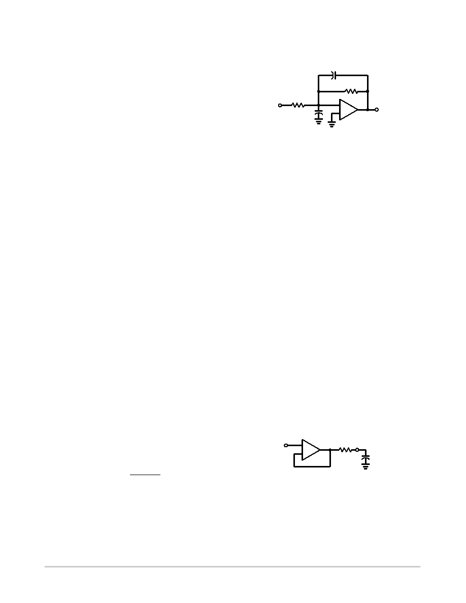
The ultra low input bias current of the NCS2001 allows
the use of extremely high value source and feedback resistor
without reducing the amplifier’s gain accuracy. These high
value resistors, in conjunction with the device input and
printed circuit board parasitic capacitances Cin, will add an
additional pole to the single pole amplifier in Figure 30. If
low enough in frequency, this additional pole can reduce the
phase margin and significantly increase the output settling
time. The effects of Cin, can be canceled by placing a zero
into the feedback loop. This is accomplished with the
addition of capacitor Cfb. An approximate value for Cfb can
be calculated by:
Cfb +
Rin
Cin
Rfb
Figure 30. Input Capacitance Pole Cancellation
+
-
Output
Rfb
Cin
Rin
Cfb
Cin = Input and printed circuit board capacitance
Input
Output
The output stage consists of complementary P and
NChannel devices connected to provide railtorail output
drive. With a 2.0 k load, the output can swing within 50 mV
of either rail. It is also capable of supplying over 75 mA
when powered from 5.0 V and 1.0 mA when powered from
0.9 V.
When connected as a unity gain follower, the NCS2001 can
directly drive capacitive loads in excess of 820 pF at room
temperature without oscillating but with significantly
reduced phase margin. The unity gain follower configuration
exhibits the highest bandwidth and is most prone to
oscillations when driving a high value capacitive load. The
capacitive load in combination with the amplifier’s output
impedance, creates a phase lag that can result in an
underdamped pulse response or a continuous oscillation.
Figure 32 shows the effect of driving a large capacitive load
in a voltage follower type of setup. When driving capacitive
loads exceeding 820 pF, it is recommended to place a low
value isolation resistor between the output of the op amp and
the load, as shown in Figure 31. The series resistor isolates the
capacitive load from the output and enhances the phase
margin. Refer to Figure 33. Larger values of R will result in
a cleaner output waveform but excessively large values will
degrade the large signal rise and fall time and reduce the
output amplitude. Depending upon the capacitor
characteristics, the isolation resistor value will typically be
between 50 to 500
W. The output drive capability for resistive
Figure 31. Capacitance Load Isolation
+
-
Output
R
Isolation resistor R = 50 to 500
CL
Input
Note that the lowest phase margin is observed at cold
temperature and low supply voltage.
相关PDF资料 |
PDF描述 |
|---|---|
| 77313-157-72 | HDR STR DR .100 DP |
| 62056-6 | CONN RCPT FLG FAST 12-18AWG .250 |
| 77319-804-72 | HDR RA DR .100 DP |
| 62026-2 | CONN RCPT/TAB FAST 16-20AWG.187 |
| 77311-822-10 | HDR STR SR .100 GDP |
相关代理商/技术参数 |
参数描述 |
|---|---|
| NCV2001SQ2T2G | 功能描述:运算放大器 - 运放 ANA SINGL OP AMP 1V 1MHZ RoHS:否 制造商:STMicroelectronics 通道数量:4 共模抑制比(最小值):63 dB 输入补偿电压:1 mV 输入偏流(最大值):10 pA 工作电源电压:2.7 V to 5.5 V 安装风格:SMD/SMT 封装 / 箱体:QFN-16 转换速度:0.89 V/us 关闭:No 输出电流:55 mA 最大工作温度:+ 125 C 封装:Reel |
| NCV2002 | 制造商:ONSEMI 制造商全称:ON Semiconductor 功能描述:Sub-One Volt Rail-to-Rail Operational Amplifier with Enable Feature |
| NCV2002SN1T1 | 功能描述:运算放大器 - 运放 0.9-7V Sngl Rail to RoHS:否 制造商:STMicroelectronics 通道数量:4 共模抑制比(最小值):63 dB 输入补偿电压:1 mV 输入偏流(最大值):10 pA 工作电源电压:2.7 V to 5.5 V 安装风格:SMD/SMT 封装 / 箱体:QFN-16 转换速度:0.89 V/us 关闭:No 输出电流:55 mA 最大工作温度:+ 125 C 封装:Reel |
| NCV2002SN1T1G | 功能描述:运算放大器 - 运放 0.9-7V Sngl Rail to Rail Extended Temp RoHS:否 制造商:STMicroelectronics 通道数量:4 共模抑制比(最小值):63 dB 输入补偿电压:1 mV 输入偏流(最大值):10 pA 工作电源电压:2.7 V to 5.5 V 安装风格:SMD/SMT 封装 / 箱体:QFN-16 转换速度:0.89 V/us 关闭:No 输出电流:55 mA 最大工作温度:+ 125 C 封装:Reel |
| NCV2002SN2T1 | 功能描述:运算放大器 - 运放 0.9-7V Sngl Rail to RoHS:否 制造商:STMicroelectronics 通道数量:4 共模抑制比(最小值):63 dB 输入补偿电压:1 mV 输入偏流(最大值):10 pA 工作电源电压:2.7 V to 5.5 V 安装风格:SMD/SMT 封装 / 箱体:QFN-16 转换速度:0.89 V/us 关闭:No 输出电流:55 mA 最大工作温度:+ 125 C 封装:Reel |
发布紧急采购,3分钟左右您将得到回复。