- 您现在的位置:买卖IC网 > PDF目录19292 > NCV2951ACD-3.3R2 (ON Semiconductor)IC REG LDO 3.3V .1A 8SOIC PDF资料下载
参数资料
| 型号: | NCV2951ACD-3.3R2 |
| 厂商: | ON Semiconductor |
| 文件页数: | 10/22页 |
| 文件大小: | 0K |
| 描述: | IC REG LDO 3.3V .1A 8SOIC |
| 产品变化通告: | Product Obsolescence 11/Feb/2009 |
| 标准包装: | 2,500 |
| 稳压器拓扑结构: | 正,固定式 |
| 输出电压: | 3.3V |
| 输入电压: | 最高 30V |
| 电压 - 压降(标准): | 0.35V @ 100mA |
| 稳压器数量: | 1 |
| 电流 - 输出: | 100mA |
| 工作温度: | -40°C ~ 125°C |
| 安装类型: | 表面贴装 |
| 封装/外壳: | 8-SOIC(0.154",3.90mm 宽) |
| 供应商设备封装: | 8-SOICN |
| 包装: | 带卷 (TR) |
| 其它名称: | NCV2951ACD-3.3R2OS NCV2951ACD-3.3R2OS-N NCV2951ACD3.3R2OS |
�� �
�
�LP2950,� LP2951,� NCV2951�
�V� in�
�for� reducing� noise� on� the� 3� lead� LP2950.� However,�
�8�
�V� in�
�V� out�
�C�
�[�
�Error�
�Output�
�Shutdown�
�Input�
�100� k�
�5�
�Error�
�SNS�
�3�
�SD� V� O� T�
�GND� FB�
�4� 7�
�1�
�2�
�NC�
�6� NC�
�R1�
�R� 2�
�0.01� m� F�
�V� out�
�1.23� to� 30� V�
�3.3� m� F�
�increasing� the� capacitor� from� 1.0� m� F� to� 220� m� F� only�
�decreases� the� noise� from� 430� m� V� to� 160� m� Vrms� for� a� 100� kHz�
�bandwidth� at� the� 5.0� V� output.�
�Noise� can� be� reduced� fourfold� by� a� bypass� capacitor�
�across� R1,� since� it� reduces� the� high� frequency� gain� from� 4�
�to� unity.� Pick�
�1�
�Bypass� 2� p� R1� x� 200� Hz�
�or� about� 0.01� m� F.� When� doing� this,� the� output� capacitor� must�
�be� increased� to� 3.3� m� F� to� maintain� stability.� These� changes�
�reduce� the� output� noise� from� 430� m� V� to� 126� m� Vrms� for� a�
�100� kHz� bandwidth� at� 5.0� V� output.� With� bypass�
�capacitor� added,� noise� no� longer� scales� with� output� voltage�
�so� that� improvements� are� more� dramatic� at� higher� output�
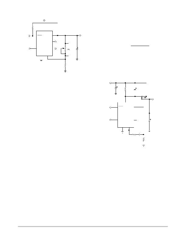
�Figure� 19.� Adjustable� Regulator�
�voltages.�
�V� +� V� (� 1� )� R1� R2� )� )� I� R1�
�The� complete� equation� for� the� output� voltage� is:�
�out� ref� FB�
�Unregulated�
�Input�
�1.0� m� F�
�10� k�
�0.01� m� F�
�MTB23P06E�
�V� in�
�5� Error�
�V� out�
�SD�
�where� V� ref� is� the� nominal� 1.235� V� reference� voltage� and� I� FB�
�is� the� feedback� pin� bias� current,� nominally� ?� 20� nA.� The�
�minimum� recommended� load� current� of� 1.0� m� A� forces� an�
�upper� limit� of� 1.2� M� W� on� the� value� of� R2,� if� the� regulator�
�must� work� with� no� load.� I� FB� will� produce� a� 2%� typical� error�
�in� V� out� which� may� be� eliminated� at� room� temperature� by�
�adjusting� R1.� For� better� accuracy,� choosing� R2� =� 100� k�
�reduces� this� error� to� 0.17%� while� increasing� the� resistor�
�program� current� to� 12� m� A.� Since� the� LP2951� typically� draws�
�75� m� A� at� no� load� with� Pin� 2� open� circuited,� the� extra� 12� m� A�
�of� current� drawn� is� often� a� worthwhile� tradeoff� for�
�eliminating� the� need� to� set� output� voltage� in� test.�
�Output� Noise�
�Error�
�Output�
�Shutdown�
�Input�
�3� 6�
�8�
�1�
�2�
�SNS�
�LP2951CN�
�V� O� T�
�GND� FB�
�4� 7�
�0.002� m� F�
�1.0� M�
�2.0� k�
�V� out�
�5.0� V� ?� 1.0%�
�0� to� 1.0� A�
�220� m� F�
�In� many� applications� it� is� desirable� to� reduce� the� noise�
�present� at� the� output.� Reducing� the� regulator� bandwidth� by�
�increasing� the� size� of� the� output� capacitor� is� the� only� method�
�Figure� 20.� 1.0� A� Regulator� with� 1.2� V� Dropout�
�http://onsemi.com�
�10�
�相关PDF资料 |
PDF描述 |
|---|---|
| TPSD107M010Y0050 | CAP TANT 100UF 10V 20% 2917 |
| 745784-4 | CONN D-SUB RCPT R/A 37POS PCB AU |
| VJ1206A181KBBAT4X | CAP CER 180PF 100V 10% NP0 1206 |
| VE-B7Z-CY-S | CONVERTER MOD DC/DC 2V 20W |
| RB-1505D | CONV DC/DC 1W 15VIN +/-05VOUT |
相关代理商/技术参数 |
参数描述 |
|---|---|
| NCV2951ACDR2 | 功能描述:低压差稳压器 - LDO 1.25-29V ADJ 100mA RoHS:否 制造商:Texas Instruments 最大输入电压:36 V 输出电压:1.4 V to 20.5 V 回动电压(最大值):307 mV 输出电流:1 A 负载调节:0.3 % 输出端数量: 输出类型:Fixed 最大工作温度:+ 125 C 安装风格:SMD/SMT 封装 / 箱体:VQFN-20 |
| NCV2951ACDR2G | 功能描述:低压差稳压器 - LDO 1.25-29V ADJ 100mA w/Error Flag RoHS:否 制造商:Texas Instruments 最大输入电压:36 V 输出电压:1.4 V to 20.5 V 回动电压(最大值):307 mV 输出电流:1 A 负载调节:0.3 % 输出端数量: 输出类型:Fixed 最大工作温度:+ 125 C 安装风格:SMD/SMT 封装 / 箱体:VQFN-20 |
| NCV2951CDR2 | 功能描述:低压差稳压器 - LDO 1.25-29V ADJ 100mA RoHS:否 制造商:Texas Instruments 最大输入电压:36 V 输出电压:1.4 V to 20.5 V 回动电压(最大值):307 mV 输出电流:1 A 负载调节:0.3 % 输出端数量: 输出类型:Fixed 最大工作温度:+ 125 C 安装风格:SMD/SMT 封装 / 箱体:VQFN-20 |
| NCV2951CDR2G | 功能描述:低压差稳压器 - LDO 1.25-29V ADJ 100mA w/Error Flag RoHS:否 制造商:Texas Instruments 最大输入电压:36 V 输出电压:1.4 V to 20.5 V 回动电压(最大值):307 mV 输出电流:1 A 负载调节:0.3 % 输出端数量: 输出类型:Fixed 最大工作温度:+ 125 C 安装风格:SMD/SMT 封装 / 箱体:VQFN-20 |
| NCV299HW1 | 制造商:ON Semiconductor 功能描述:DARLINGTON LAMP DRIVER - Bulk |
发布紧急采购,3分钟左右您将得到回复。