- 您现在的位置:买卖IC网 > PDF目录20172 > NCV2951ACD3.3R2G (ON Semiconductor)IC REG LDO 3.3V .1A 8-SOIC PDF资料下载
参数资料
| 型号: | NCV2951ACD3.3R2G |
| 厂商: | ON Semiconductor |
| 文件页数: | 9/22页 |
| 文件大小: | 0K |
| 描述: | IC REG LDO 3.3V .1A 8-SOIC |
| 标准包装: | 2,500 |
| 稳压器拓扑结构: | 正,固定式 |
| 输出电压: | 3.3V |
| 输入电压: | 最高 30V |
| 电压 - 压降(标准): | 0.35V @ 100mA |
| 稳压器数量: | 1 |
| 电流 - 输出: | 100mA |
| 工作温度: | -40°C ~ 125°C |
| 安装类型: | 表面贴装 |
| 封装/外壳: | 8-SOIC(0.154",3.90mm 宽) |
| 供应商设备封装: | 8-SOICN |
| 包装: | 带卷 (TR) |
�� �
�
�LP2950,� LP2951,� NCV2951�
�APPLICATIONS� INFORMATION�
�Introduction�
�The� LP2950/LP2951� regulators� are� designed� with�
�internal� current� limiting� and� thermal� shutdown� making� them�
�user� ?� friendly.� Typical� application� circuits� for� the� LP2950�
�and� LP2951� are� shown� in� Figures� 20� through� 28.�
�These� regulators� are� not� internally� compensated� and� thus�
�require� a� 1.0� m� F� (or� greater)� capacitance� between� the�
�LP2950/LP2951� output� terminal� and� ground� for� stability.�
�Most� types� of� aluminum,� tantalum� or� multilayer� ceramic�
�will� perform� adequately.� Solid� tantalums� or� appropriate�
�multilayer� ceramic� capacitors� are� recommended� for�
�operation� below� 25� ?� C.�
�At� lower� values� of� output� current,� less� output� capacitance�
�is� required� for� output� stability.� The� capacitor� can� be� reduced�
�to� 0.33� m� F� for� currents� less� than� 10� mA,� or� 0.1� m� F� for� currents�
�below� 1.0� mA.� Using� the� 8� pin� versions� at� voltages� less� than�
�5.0� V� operates� the� error� amplifier� at� lower� values� of� gain,� so�
�that� more� output� capacitance� is� needed� for� stability.� For� the�
�worst� case� operating� condition� of� a� 100� mA� load� at� 1.23� V�
�output� (output� Pin� 1� connected� to� the� feedback� Pin� 7)� a�
�minimum� capacitance� of� 3.3� m� F� is� recommended.�
�The� LP2950� will� remain� stable� and� in� regulation� when�
�operated� with� no� output� load.� When� setting� the� output�
�to� the� LP2951� is� ramped� up� and� down.� The� ERROR� signal�
�becomes� valid� (low)� at� about� 1.3� V� input.� It� goes� high� when�
�the� input� reaches� about� 5.0� V� (V� out� exceeds� about� 4.75� V).�
�Since� the� LP2951’s� dropout� voltage� is� dependent� upon� the�
�load� current� (refer� to� the� curve� in� the� Typical� Performance�
�Characteristics),� the� input� voltage� trip� point� will� vary� with�
�load� current.� The� output� voltage� trip� point� does� not� vary�
�with� load.�
�The� error� comparator� output� is� an� open� collector� which�
�requires� an� external� pullup� resistor.� This� resistor� may� be�
�returned� to� the� output� or� some� other� voltage� within� the�
�system.� The� resistance� value� should� be� chosen� to� be�
�consistent� with� the� 400� m� A� sink� capability� of� the� error�
�comparator.� A� value� between� 100� k� and� 1.0� M� W� is�
�suggested.� No� pullup� resistance� is� required� if� this� output� is�
�unused.�
�When� operated� in� the� shutdown� mode,� the� error�
�comparator� output� will� go� high� if� it� has� been� pulled� up� to� an�
�external� supply.� To� avoid� this� invalid� response,� the� error�
�comparator� output� should� be� pulled� up� to� V� out� (see�
�Figure� 18).�
�5.0� V�
�voltage� of� the� LP2951� with� external� resistors,� the� resistance�
�values� should� be� chosen� to� draw� a� minimum� of� 1.0� m� A.�
�A� bypass� capacitor� is� recommended� across� the�
�Output�
�Voltage�
�4.75� V�
�4.70� V�
�LP2950/LP2951� input� to� ground� if� more� than� 4� inches� of�
�wire� connects� the� input� to� either� a� battery� or� power� supply�
�filter� capacitor.�
�Input� capacitance� at� the� LP2951� Feedback� Pin� 7� can�
�create� a� pole,� causing� instability� if� high� value� external�
�resistors� are� used� to� set� the� output� voltage.� Adding� a� 100� pF�
�capacitor� between� the� Output� Pin� 1� and� the� Feedback� Pin� 7�
�and� increasing� the� output� filter� capacitor� to� at� least� 3.3� m� F�
�will� stabilize� the� feedback� loop.�
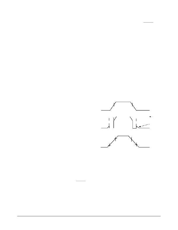
�ERROR�
�Input�
�Voltage�
�Not�
�Valid�
�1.3� V�
�4.75� V� +� V� dropout�
�Not�
�Valid�
�4.70� V� +� V� dropout�
�1.3� V�
�Pullup�
�to� Ext�
�Pullup�
�to� V� out�
�Error� Detection� Comparator�
�The� comparator� switches� to� a� positive� logic� low� whenever�
�the� LP2951� output� voltage� falls� more� than� approximately�
�5.0%� out� of� regulation.� This� value� is� the� comparator� ’s�
�designed� ?� in� offset� voltage� of� 60� mV� divided� by� the� 1.235� V�
�internal� reference.� As� shown� in� the� representative� block�
�diagram.� This� trip� level� remains� 5.0%� below� normal�
�regardless� of� the� value� of� regulated� output� voltage.� For�
�example,� the� error� flag� trip� level� is� 4.75� V� for� a� normal� 5.0� V�
�regulated� output,� or� 9.50� V� for� a� 10� V� output� voltage.�
�Figure� 2� is� a� timing� diagram� which� shows� the� ERROR�
�signal� and� the� regulated� output� voltage� as� the� input� voltage�
�Figure� 18.� ERROR� Output� Timing�
�Programming� the� Output� Voltage� (LP2951)�
�The� LP2951CX� may� be� pin� ?� strapped� for� the� nominal�
�fixed� output� voltage� using� its� internal� voltage� divider� by�
�tying� Pin� 1� (output)� to� Pin� 2� (sense)� and� Pin� 7� (feedback)� to�
�Pin� 6� (5.0� V� tap).� Alternatively,� it� may� be� programmed� for�
�any� output� voltage� between� its� 1.235� reference� voltage� and�
�its� 30� V� maximum� rating.� An� external� pair� of� resistors� is�
�required,� as� shown� in� Figure� 19.�
�http://onsemi.com�
�9�
�相关PDF资料 |
PDF描述 |
|---|---|
| EMC35DRTH-S93 | CONN EDGECARD 70POS DIP .100 SLD |
| IDT71V424L10PH8 | IC SRAM 4MBIT 10NS 44TSOP |
| T86D685K035ESAL | CAP TANT 6.8UF 35V 10% 2917 |
| RZE30DHAS | CONN EDGE DUAL 1MM R/A 60 POS |
| T86D226M025ESAL | CAP TANT 22UF 25V 20% 2917 |
相关代理商/技术参数 |
参数描述 |
|---|---|
| NCV2951ACDR2 | 功能描述:低压差稳压器 - LDO 1.25-29V ADJ 100mA RoHS:否 制造商:Texas Instruments 最大输入电压:36 V 输出电压:1.4 V to 20.5 V 回动电压(最大值):307 mV 输出电流:1 A 负载调节:0.3 % 输出端数量: 输出类型:Fixed 最大工作温度:+ 125 C 安装风格:SMD/SMT 封装 / 箱体:VQFN-20 |
| NCV2951ACDR2G | 功能描述:低压差稳压器 - LDO 1.25-29V ADJ 100mA w/Error Flag RoHS:否 制造商:Texas Instruments 最大输入电压:36 V 输出电压:1.4 V to 20.5 V 回动电压(最大值):307 mV 输出电流:1 A 负载调节:0.3 % 输出端数量: 输出类型:Fixed 最大工作温度:+ 125 C 安装风格:SMD/SMT 封装 / 箱体:VQFN-20 |
| NCV2951CDR2 | 功能描述:低压差稳压器 - LDO 1.25-29V ADJ 100mA RoHS:否 制造商:Texas Instruments 最大输入电压:36 V 输出电压:1.4 V to 20.5 V 回动电压(最大值):307 mV 输出电流:1 A 负载调节:0.3 % 输出端数量: 输出类型:Fixed 最大工作温度:+ 125 C 安装风格:SMD/SMT 封装 / 箱体:VQFN-20 |
| NCV2951CDR2G | 功能描述:低压差稳压器 - LDO 1.25-29V ADJ 100mA w/Error Flag RoHS:否 制造商:Texas Instruments 最大输入电压:36 V 输出电压:1.4 V to 20.5 V 回动电压(最大值):307 mV 输出电流:1 A 负载调节:0.3 % 输出端数量: 输出类型:Fixed 最大工作温度:+ 125 C 安装风格:SMD/SMT 封装 / 箱体:VQFN-20 |
| NCV299HW1 | 制造商:ON Semiconductor 功能描述:DARLINGTON LAMP DRIVER - Bulk |
发布紧急采购,3分钟左右您将得到回复。