参数资料
| 型号: | NCV33204DR2G |
| 厂商: | ON Semiconductor |
| 文件页数: | 18/18页 |
| 文件大小: | 0K |
| 描述: | IC OPAMP QUAD R-R LO VOLT 14SOIC |
| 标准包装: | 1 |
| 放大器类型: | 通用 |
| 电路数: | 4 |
| 输出类型: | 满摆幅 |
| 转换速率: | 1 V/µs |
| 增益带宽积: | 2.2MHz |
| 电流 - 输入偏压: | 80nA |
| 电压 - 输入偏移: | 10000µV |
| 电流 - 电源: | 1.125mA |
| 电流 - 输出 / 通道: | 80mA |
| 电压 - 电源,单路/双路(±): | 1.8 V ~ 12 V,±0.9 V ~ 6 V |
| 工作温度: | -55°C ~ 125°C |
| 安装类型: | 表面贴装 |
| 封装/外壳: | 14-SOIC(0.154",3.90mm 宽) |
| 供应商设备封装: | 14-SOICN |
| 包装: | 剪切带 (CT) |
| 其它名称: | NCV33204DR2GOSCT |
MC33201, MC33202, MC33204, NCV33202, NCV33204
http://onsemi.com
9
DETAILED OPERATING DESCRIPTION
General Information
The MC33201/2/4 family of operational amplifiers are
unique in their ability to swing railtorail on both the input
and the output with a completely bipolar design. This offers
low noise, high output current capability and a wide
common mode input voltage range even with low supply
voltages. Operation is guaranteed over an extended
temperature range and at supply voltages of 2.0 V, 3.3 V and
5.0 V and ground.
Since the common mode input voltage range extends from
VCC to VEE, it can be operated with either single or split
voltage supplies. The MC33201/2/4 are guaranteed not to
latch or phase reverse over the entire common mode range,
however, the inputs should not be allowed to exceed
maximum ratings.
Circuit Information
Railtorail performance is achieved at the input of the
amplifiers by using parallel NPNPNP differential input
stages. When the inputs are within 800 mV of the negative
rail, the PNP stage is on. When the inputs are more than 800
mV greater than VEE, the NPN stage is on. This switching of
input pairs will cause a reversal of input bias currents (see
Figure 6). Also, slight differences in offset voltage may be
noted between the NPN and PNP pairs. Crosscoupling
techniques have been used to keep this change to a minimum.
In addition to its railtorail performance, the output stage
is current boosted to provide 80 mA of output current,
enabling the op amp to drive 600
W loads. Because of this
high output current capability, care should be taken not to
exceed the 150
°C maximum junction temperature.
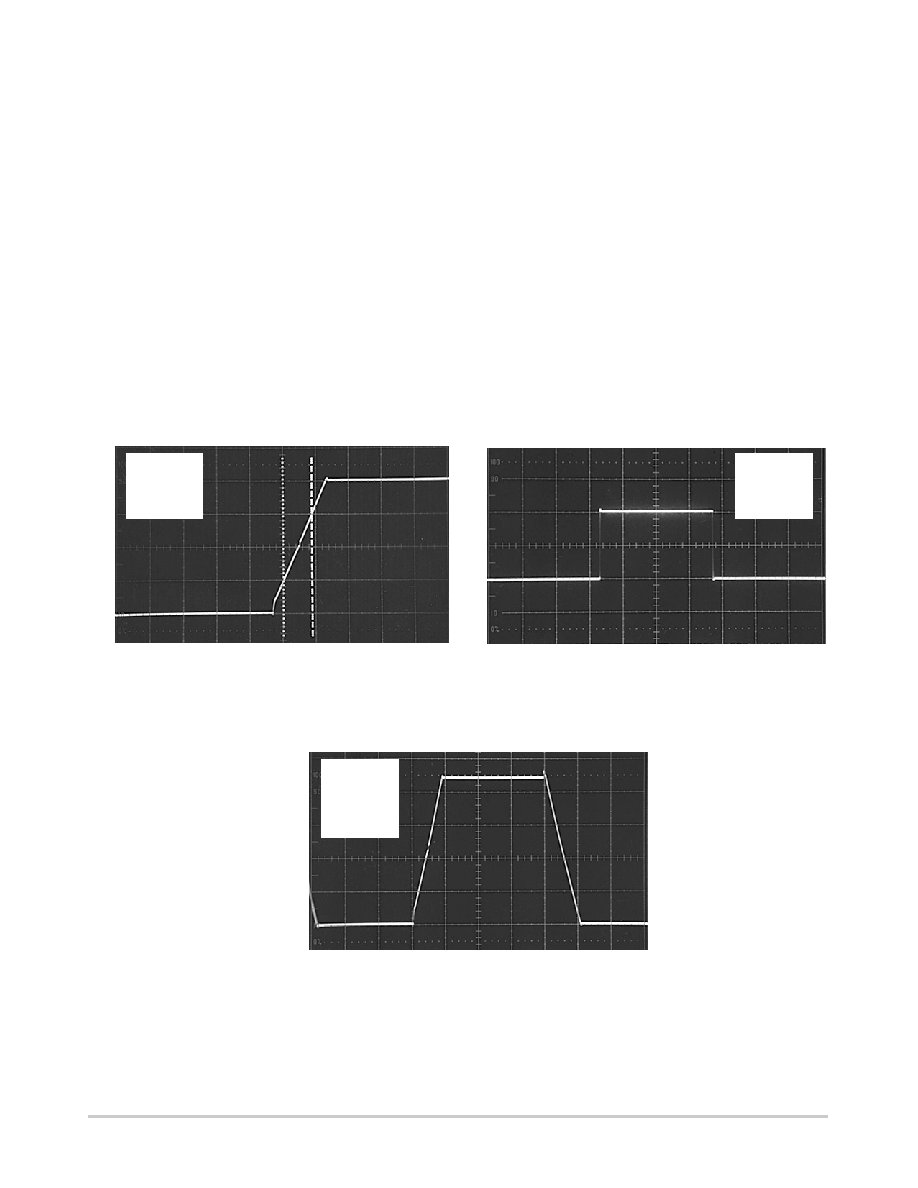
O
,OUTPUT
VOL
TAGE
(50
mV/DIV)
V
t, TIME (10
ms/DIV)
Figure 26. Noninverting Amplifier Slew Rate
Figure 27. Small Signal Transient Response
t, TIME (5.0
ms/DIV)
Figure 28. Large Signal Transient Response
VCC = +6.0 V
VEE = -6.0 V
RL = 600 W
CL = 100 pF
TA = 25°C
O
,OUTPUT
VOL
TAGE
(2.0
mV/DIV)
VCC = +6.0 V
VEE = -6.0 V
RL = 600 W
CL = 100 pF
AV = 1.0
TA = 25°C
V
VCC = +6.0 V
VEE = -6.0 V
RL = 600 W
CL = 100 pF
TA = 25°C
t, TIME (10
ms/DIV)
O
,OUTPUT
VOL
TAGE
(2.0
V/DIV)
V
Surface mount board layout is a critical portion of the total
design. The footprint for the semiconductor packages must be
the correct size to ensure proper solder connection interface
between the board and the package. With the correct pad
geometry, the packages will selfalign when subjected to a
solder reflow process.
相关PDF资料 |
PDF描述 |
|---|---|
| 98414-S06-44ULF | MINITEK |
| 66L090 | THERMOSTAT 90 DEG NC 8-DIP |
| 1-160759-2 | CONN RCPT POS LOC 20-16AWG .250 |
| 63038-2 | CONN TAB FASTON .250 BRASS |
| 961126-6700-AR-PT | CONN HEADER VERT 26POS GOLD SMD |
相关代理商/技术参数 |
参数描述 |
|---|---|
| NCV33204DTBR2 | 功能描述:运算放大器 - 运放 1.8-12V Quad Rail to RoHS:否 制造商:STMicroelectronics 通道数量:4 共模抑制比(最小值):63 dB 输入补偿电压:1 mV 输入偏流(最大值):10 pA 工作电源电压:2.7 V to 5.5 V 安装风格:SMD/SMT 封装 / 箱体:QFN-16 转换速度:0.89 V/us 关闭:No 输出电流:55 mA 最大工作温度:+ 125 C 封装:Reel |
| NCV33204DTBR2G | 功能描述:运算放大器 - 运放 1.8-12V Quad Rail to Rail -55 to 125 Cel RoHS:否 制造商:STMicroelectronics 通道数量:4 共模抑制比(最小值):63 dB 输入补偿电压:1 mV 输入偏流(最大值):10 pA 工作电源电压:2.7 V to 5.5 V 安装风格:SMD/SMT 封装 / 箱体:QFN-16 转换速度:0.89 V/us 关闭:No 输出电流:55 mA 最大工作温度:+ 125 C 封装:Reel |
| NCV33269 | 制造商:ONSEMI 制造商全称:ON Semiconductor 功能描述:AC-DC Offline Switching Controllers/Regulators |
| NCV33269D | 制造商:ONSEMI 制造商全称:ON Semiconductor 功能描述:800 mA, Adjustable Output, Low Dropout Voltage Regulator |
| NCV33269DR2G | 功能描述:低压差控制器 - LDO 800 MA, ADJUSTABLE 1.35-1 RoHS:否 制造商:Micrel 最大输入电压:5.5 V 输出电压:Adjustable 输出电流:10 mA 负载调节: 输出类型:Adjustable, Fixed 输出端数量:1 最大工作温度:+ 125 C 安装风格:SMD/SMT 封装 / 箱体:SOT-23-6 |
发布紧急采购,3分钟左右您将得到回复。