- 您现在的位置:买卖IC网 > PDF目录19987 > NCV4279A50D2R2G (ON Semiconductor)IC REG LDO 5V 14SOIC PDF资料下载
参数资料
| 型号: | NCV4279A50D2R2G |
| 厂商: | ON Semiconductor |
| 文件页数: | 12/15页 |
| 文件大小: | 0K |
| 描述: | IC REG LDO 5V 14SOIC |
| 标准包装: | 1 |
| 稳压器拓扑结构: | 正,固定式 |
| 输出电压: | 5V |
| 输入电压: | 最高 45 V |
| 电压 - 压降(标准): | 0.25V @ 100mA |
| 稳压器数量: | 1 |
| 电流 - 限制(最小): | 150mA |
| 工作温度: | -40°C ~ 125°C |
| 安装类型: | 表面贴装 |
| 封装/外壳: | 14-SOIC(0.154",3.90mm 宽) |
| 供应商设备封装: | 14-SOICN |
| 包装: | 标准包装 |
| 其它名称: | NCV4279A50D2R2GOSDKR |
�� �
�
�NCV4279A�
�SENSE� INPUT� (SI)� /� SENSE� OUTPUT� (SO)� VOLTAGE�
�MONITOR�
�An� on� ?� chip� comparator� is� available� to� provide� early�
�warning� to� the� microprocessor� of� a� possible� reset� signal.� The�
�output� is� from� an� open� collector� driver.� The� reset� signal�
�typically� turns� the� microprocessor� off� instantaneously.� This�
�can� cause� unpredictable� results� with� the� microprocessor.�
�The� signal� received� from� the� SO� pin� will� allow� the�
�microprocessor� time� to� complete� its� present� task� before�
�shutting� down.� This� function� is� performed� by� a� comparator�
�referenced� to� the� band� gap� voltage.� The� actual� trip� point� can�
�be� programmed� externally� using� a� resistor� divider� to� the�
�input� monitor� SI� (Figure� 20).� The� values� for� R� SI1� and� R� SI2�
�are� selected� for� a� typical� threshold� of� 1.20� V� on� the� SI� Pin.�
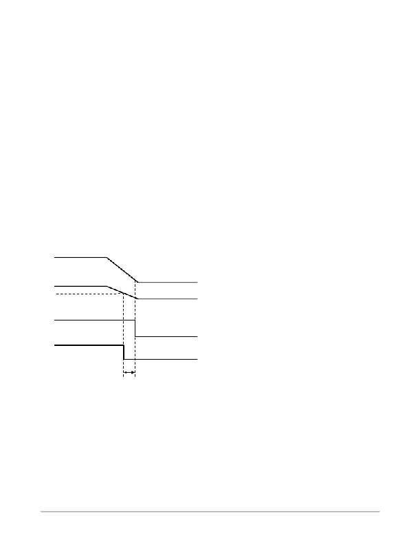
�SIGNAL� OUTPUT�
�Figure� 21� shows� the� SO� Monitor� timing� waveforms� as� a�
�result� of� the� circuit� depicted� in� Figure� 20.� As� the� output�
�voltage� (V� Q� )� falls,� the� monitor� threshold� (V� SILOW� ),� is�
�crossed.� This� causes� the� voltage� on� the� SO� output� to� go� low�
�sending� a� warning� signal� to� the� microprocessor� that� a� reset�
�signal� may� occur� in� a� short� period� of� time.� T� WARNING� is� the�
�time� the� microprocessor� has� to� complete� the� function� it� is�
�currently� working� on� and� get� ready� for� the� reset�
�shutdown� signal.� When� the� voltage� on� the� SO� goes� low� and�
�the� RO� stays� high� the� current� consumption� is� typically�
�560� m� A� at� 1� mA� load� current.�
�V� Q�
�SI�
�V� SI,Low�
�V� RO�
�SO�
�T� WARNING�
�Figure� 21.� SO� Warning� Waveform� Time� Diagram�
�STABILITY� CONSIDERATIONS�
�The� input� capacitor� C� I� in� Figure� 20� is� necessary� for�
�compensating� input� line� reactance.� Possible� oscillations�
�caused� by� input� inductance� and� input� capacitance� can� be�
�damped� by� using� a� resistor� of� approximately� 1.0� W� in� series�
�with� C� I.�
�The� output� or� compensation� capacitor� helps� determine�
�three� main� characteristics� of� a� linear� regulator:� startup� delay,�
�load� transient� response� and� loop� stability.�
�The� capacitor� value� and� type� should� be� based� on� cost,�
�availability,� size� and� temperature� constraints.� The�
�aluminum� electrolytic� capacitor� is� the� least� expensive�
�solution,� but,� if� the� circuit� operates� at� low� temperatures�
�(� ?� 25� °� C� to� ?� 40� °� C),� both� the� value� and� ESR� of� the� capacitor�
�will� vary� considerably.� The� capacitor� manufacturer� ’s� data�
�sheet� usually� provides� this� information.�
�The� 10� m� F� output� capacitor� C� Q� shown� in� Figure� 20� should�
�work� for� most� applications;� however,� it� is� not� necessarily� the�
�optimized� solution.� Stability� is� guaranteed� at� CQ� is� min�
�2.2� m� F� and� max� ESR� is� 10� W� .� There� is� no� min� ESR� limit�
�which� was� proved� with� MURATA’s� ceramic� caps�
�GRM31MR71A225KA01� (2.2� m� F,� 10� V,� X7R,� 1206)� and�
�GRM31CR71A106KA01� (10� m� F,� 10� V,� X7R,� 1206)� directly�
�soldered� between� output� and� ground� pins.�
�CALCULATING� POWER� DISSIPATION� IN� A� SINGLE�
�OUTPUT� LINEAR� REGULATOR�
�The� maximum� power� dissipation� for� a� single� output�
�regulator� (Figure� 20)� is:�
�PD(max)� +� [VI(max)� *� VQ(min)]� IQ(max)� )� VI(max)� Iq� (eq.� 4)�
�where:�
�V� I(max)� is� the� maximum� input� voltage,�
�V� Q(min)� is� the� minimum� output� voltage,�
�I� Q(max)� is� the� maximum� output� current� for� the� application,�
�and� I� q� is� the� quiescent� current� the� regulator� consumes� at�
�I� Q(max)� .�
�Once� the� value� of� P� D(max)� is� known,� the� maximum�
�permissible� value� of� R� q� JA� can� be� calculated:�
�R� q� JA� =� (150� °� C� –� T� A� )� /� P� D� (eq.� 5)�
�The� value� of� R� q� JA� can� then� be� compared� with� those� in� the�
�package� section� of� the� data� sheet.� Those� packages� with� R� q� JA� ’s�
�less� than� the� calculated� value� in� equation� 2� will� keep� the� die�
�temperature� below� 150� °� C.� In� some� cases,� none� of� the� packages�
�will� be� sufficient� to� dissipate� the� heat� generated� by� the� IC,� and�
�an� external� heatsink� will� be� required.� The� current� flow� and�
�voltages� are� shown� in� the� Measurement� Circuit� Diagram.�
�HEATSINKS�
�A� heatsink� effectively� increases� the� surface� area� of� the�
�package� to� improve� the� flow� of� heat� away� from� the� IC� and�
�into� the� surrounding� air.�
�Each� material� in� the� heat� flow� path� between� the� IC� and� the�
�outside� environment� will� have� a� thermal� resistance.� Like�
�series� electrical� resistances,� these� resistances� are� summed� to�
�determine� the� value� of� R� q� JA� :�
�R� q� JA� +� R� q� JC� )� R� q� CS� )� R� q� SA� (eq.� 6)�
�where:�
�R� q� JC� =� the� junction� ?� to� ?� case� thermal� resistance,�
�R� q� CS� =� the� case� ?� to� ?� heat� sink� thermal� resistance,� and�
�R� q� SA� =� the� heat� sink� ?� to� ?� ambient� thermal� resistance.�
�R� q� JC� appears� in� the� package� section� of� the� data� sheet.� Like�
�R� q� JA� ,� it� too� is� a� function� of� package� type.� R� q� CS� and� R� q� SA� are�
�functions� of� the� package� type,� heatsink� and� the� interface�
�between� them.� These� values� appear� in� data� sheets� of�
�heatsink� manufacturers.� Thermal,� mounting,� and�
�heatsinking� considerations� are� discussed� in� the�
�ON� Semiconductor� application� note� AN1040/D,� available�
�on� the� ON� Semiconductor� website.�
�http://onsemi.com�
�12�
�相关PDF资料 |
PDF描述 |
|---|---|
| VE-J7J-CY-B1 | CONVERTER MOD DC/DC 36V 50W |
| VE-25L-CW-S | CONVERTER MOD DC/DC 28V 100W |
| DS1225AD-150 | IC NVSRAM 64KBIT 150NS 28DIP |
| T86D686K016EBSL | CAP TANT 68UF 16V 10% 2917 |
| 2-5530843-0 | CONN EDGECARD 40POS .100 VERT |
相关代理商/技术参数 |
参数描述 |
|---|---|
| NCV4279B | 制造商:ONSEMI 制造商全称:ON Semiconductor 功能描述:5.0 V Micropower 150 mA LDO Linear Regulator with DELAY, Adjustable RESET, and Monitor FLAG |
| NCV4279BD1 | 制造商:ONSEMI 制造商全称:ON Semiconductor 功能描述:5.0 V Micropower 150 mA LDO Linear Regulator with DELAY, Adjustable RESET, and Monitor FLAG |
| NCV4279BD1R2 | 功能描述:IC REG LDO 5V .15A 8SOIC RoHS:否 类别:集成电路 (IC) >> PMIC - 稳压器 - 线性 系列:- 标准包装:3,000 系列:- 稳压器拓扑结构:正,固定式和可调式 输出电压:3.3V,1.25 V ~ 5.7 V 输入电压:4.5 V ~ 7 V 电压 - 压降(标准):1.1V @ 1A 稳压器数量:2 电流 - 输出:1A 电流 - 限制(最小):1A 工作温度:0°C ~ 125°C 安装类型:表面贴装 封装/外壳:TO-252-5,DPak(4 引线 + 接片),TO-252AD 供应商设备封装:PPAK 包装:管件 其它名称:497-3576-5 |
| NCV4279BD1R2G | 制造商:ON Semiconductor 功能描述:ANA 5.0V MICROPOWER, PB FREE - Tape and Reel |
| NCV4279BD2 | 制造商:ONSEMI 制造商全称:ON Semiconductor 功能描述:5.0 V Micropower 150 mA LDO Linear Regulator with DELAY, Adjustable RESET, and Monitor FLAG |
发布紧急采购,3分钟左右您将得到回复。