- 您现在的位置:买卖IC网 > PDF目录19981 > NCV4299D233G (ON Semiconductor)IC REG LDO 3.3V .15A 14-SOIC PDF资料下载
参数资料
| 型号: | NCV4299D233G |
| 厂商: | ON Semiconductor |
| 文件页数: | 16/23页 |
| 文件大小: | 0K |
| 描述: | IC REG LDO 3.3V .15A 14-SOIC |
| 标准包装: | 55 |
| 稳压器拓扑结构: | 正,固定式 |
| 输出电压: | 3.3V |
| 输入电压: | 4.4 V ~ 45 V |
| 电压 - 压降(标准): | 0.22V @ 100mA |
| 稳压器数量: | 1 |
| 电流 - 输出: | 150mA |
| 电流 - 限制(最小): | 250mA |
| 工作温度: | -40°C ~ 150°C |
| 安装类型: | 表面贴装 |
| 封装/外壳: | 14-SOIC(0.154",3.90mm 宽) |
| 供应商设备封装: | 14-SOICN |
| 包装: | 管件 |
�� �
�
�NCV4299�
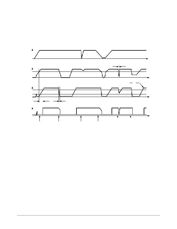
�Reset� Output� (RO)�
�A� reset� signal,� Reset� Output� (RO,� low� voltage)� is�
�generated� as� the� IC� powers� up.� After� the� output� voltage� V� Q�
�increases� above� the� reset� threshold� voltage� V� RT� ,� the� delay�
�timer� D� is� started.� When� the� voltage� on� the� delay� timer� V� D�
�passes� V� UD� ,� the� reset� signal� RO� goes� high.� A� discharge� of�
�the� delay� timer� (V� D� )� is� started� when� V� Q� drops� and� stays�
�below� the� reset� threshold� voltage� V� RT� .� When� the� voltage� of�
�the� delay� timer� (V� D� )� drops� below� the� lower� threshold�
�voltage� V� LD� ,� the� reset� output� voltage� V� RO� is� brought� low� to�
�reset� the� processor.�
�The� reset� output� RO� is� an� open� collector� NPN� transistor,�
�controlled� by� a� low� voltage� detection� circuit.� The� circuit� is�
�functionally� independent� of� the� rest� of� the� IC,� thereby�
�guaranteeing� that� RO� is� valid� for� V� Q� as� low� as� 1.0� V.�
�V� I�
�t�
�V� Q�
�<� t� RR�
�V� RT�
�t�
�+� D�
�V� D�
�V� UD�
�V� LD�
�V� RO�
�V� RO,SAT�
�t� d�
�t� RR�
�dV�
�dt�
�I�
�CD�
�t�
�t�
�Power� ?� on� ?� Reset�
�Thermal�
�Shutdown�
�Voltage� Dip�
�at� Input�
�Undervoltage�
�Secondary�
�Spike�
�Overload�
�at� Output�
�Figure� 41.� Reset� Timing� Diagram�
�Reset� Adjust� (RADJ)�
�The� reset� threshold� V� RT� can� be� decreased� from� a� typical�
�value� of� 4.64� V� to� as� low� as� 3.5� V� by� using� an� external�
�voltage� divider� connected� from� the� Q� lead� to� the� pin� RADJ,�
�as� shown� in� Figures� 39� and� 40.� The� resistor� divider� keeps� the�
�voltage� above� the� V� RADJ,TH� ,� (typ.� 1.36� V),� for� the� desired�
�input� voltages� and� overrides� the� internal� threshold� detector.�
�Adjust� the� voltage� divider� according� to� the� following�
�relationship:�
�VTHRES� +� VRADJ,� TH� ·� (RADJ1� )� RADJ2)� RADJ2�
�(eq.� 1)�
�If� the� reset� adjust� option� is� not� needed,� the� RADJ� ?� pin�
�should� be� connected� to� GND� causing� the� reset� threshold� to�
�Reset� Delay� (D)�
�The� reset� delay� circuit� provides� a� delay� (programmable� by�
�capacitor� C� D� )� on� the� reset� output� RO� lead.� The� delay� lead� D�
�provides� charge� current� I� D� (typically� 7.1� m� A)� to� the� external�
�delay� capacitor� C� D� during� the� following� times:�
�1.� During� Powerup� (once� the� regulation� threshold� has�
�been� exceeded).�
�2.� After� a� reset� event� has� occurred� and� the� device�
�is� back� in� regulation.� The� delay� capacitor� is�
�set� to� discharge� when� the� regulation� (V� RT� ,� reset�
�threshold� voltage)� has� been� violated.� When�
�the� delay� capacitor� discharges� to� down� to� V� LD� ,�
�the� reset� signal� RO� pulls� low.�
�go� to� its� default� value� (typ.� 4.64� V).�
�http://onsemi.com�
�16�
�相关PDF资料 |
PDF描述 |
|---|---|
| VI-B4Z-CV-F3 | CONVERTER MOD DC/DC 2V 60W |
| VI-B4Z-CV-F2 | CONVERTER MOD DC/DC 2V 60W |
| CDRH74NP-220MC | POWER INDUCTOR 22UH 1.23A SMD |
| VI-B4Y-CV-F3 | CONVERTER MOD DC/DC 3.3V 99W |
| DS1230AB-150 | IC NVSRAM 256KBIT 150NS 28DIP |
相关代理商/技术参数 |
参数描述 |
|---|---|
| NCV4299D233R2G | 功能描述:低压差稳压器 - LDO ANA 150mA LDO REG RoHS:否 制造商:Texas Instruments 最大输入电压:36 V 输出电压:1.4 V to 20.5 V 回动电压(最大值):307 mV 输出电流:1 A 负载调节:0.3 % 输出端数量: 输出类型:Fixed 最大工作温度:+ 125 C 安装风格:SMD/SMT 封装 / 箱体:VQFN-20 |
| NCV4299D2G | 功能描述:低压差稳压器 - LDO LDO REG RoHS:否 制造商:Texas Instruments 最大输入电压:36 V 输出电压:1.4 V to 20.5 V 回动电压(最大值):307 mV 输出电流:1 A 负载调节:0.3 % 输出端数量: 输出类型:Fixed 最大工作温度:+ 125 C 安装风格:SMD/SMT 封装 / 箱体:VQFN-20 |
| NCV4299D2R2 | 功能描述:低压差稳压器 - LDO 5V 150mA Precision RoHS:否 制造商:Texas Instruments 最大输入电压:36 V 输出电压:1.4 V to 20.5 V 回动电压(最大值):307 mV 输出电流:1 A 负载调节:0.3 % 输出端数量: 输出类型:Fixed 最大工作温度:+ 125 C 安装风格:SMD/SMT 封装 / 箱体:VQFN-20 |
| NCV4299D2R2G | 功能描述:低压差稳压器 - LDO LDO REG RoHS:否 制造商:Texas Instruments 最大输入电压:36 V 输出电压:1.4 V to 20.5 V 回动电压(最大值):307 mV 输出电流:1 A 负载调节:0.3 % 输出端数量: 输出类型:Fixed 最大工作温度:+ 125 C 安装风格:SMD/SMT 封装 / 箱体:VQFN-20 |
| NCV431AIDMR2 | 功能描述:基准电压& 基准电流 2.5-36V ADJ 1-100mA RoHS:否 制造商:STMicroelectronics 产品:Voltage References 拓扑结构:Shunt References 参考类型:Programmable 输出电压:1.24 V to 18 V 初始准确度:0.25 % 平均温度系数(典型值):100 PPM / C 串联 VREF - 输入电压(最大值): 串联 VREF - 输入电压(最小值): 分流电流(最大值):60 mA 最大工作温度:+ 125 C 封装 / 箱体:SOT-23-3L 封装:Reel |
发布紧急采购,3分钟左右您将得到回复。