参数资料
| 型号: | NCV7441D20G |
| 厂商: | ON Semiconductor |
| 文件页数: | 5/10页 |
| 文件大小: | 0K |
| 描述: | IC TXRX CAN DUAL HS LP 14-SOIC |
| 标准包装: | 55 |
| 系列: | * |
| 其它名称: | NCV7441D20G-ND NCV7441D20GOS |
NCV7441
http://onsemi.com
4
If the main power supply VCC (nominal 5 V) is above its undervoltage (VCC_UV) level, each CAN channel can enter either
normal mode (when the corresponding STB1/2 digital input is pulled Low) or standby mode (when the corresponding STB1/2
signal is left High):
In the normal mode:
The bus transceiver is ready to transmit and receive CAN bus signals with the full CAN communication speed (up to
1 Mbps) and thus interconnect the CAN bus with the corresponding CAN controller through digital pins TxD1/2 and
RxD1/2
The bus pins are internally biased to typically VCC/2 through the input circuitry
TxD1/2 input pin is monitored by a timeout in order to prevent a permanent dominant being forced to the bus thus
preventing other nodes from communicating. If TxD1/2 is Low for longer than tcnt(timeout), the transmitter switches
back to recessive. Only when TxD1/2 returns to High, the timeout counter is reset and the transmitter is ready to
transmit dominant symbols again. The TxD1/2 timeout protection is implemented individually for both CAN
transceivers.
A common thermal monitoring circuit compares the circuit junction temperatures with threshold TJ(sd). If the thermal
shutdown level is exceeded, dominant transmission is disabled. The circuit remains biased and ready to transmit but
the logical path from TxD1/2 pin(s) is blocked. The transmission is again enabled when the junction temperature
decreases below the shutdown level and the TxD1/2 pin returns to the High level, thus avoiding thermal oscillations.
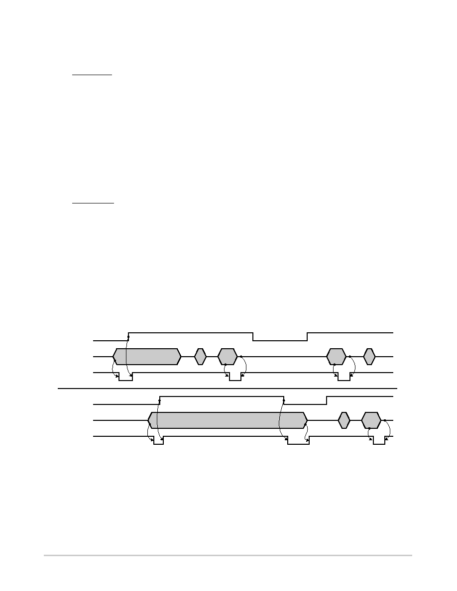
In the standby mode:
The respective transmitter is disabled and the current consumption of the channel is fundamentally reduced. Only the
lowpower receiver on the channel remains active in order to detect potential CAN bus wakeups. The logical signal
on TxD1/2 input is ignored.
The bus pins are biased to GND through the input circuitry
Digital output RxD1/2 signals the output of the lowpower receiver and can be used as a wakeup signal in the
application. A filtering time tdBUS is applied between the bus activity and the RxD1/2 signal in order to ensure that
only sufficiently long dominant signals on the bus will be propagated to the digital output. In addition, dominant bus
signals are ignored in case they were present during normaltostandby mode transition; in this way unwanted
wakeups are avoided in case of permanent dominant failure on the bus. Example waveforms illustrating bus activity
detection in standby mode are shown in Figure 3.
In order to ensure a safe device state, the digital inputs STB1/2 and TxD1/2 are connected through internal pullup resistors
to VCC thus ensuring that both channels remain in standby mode and/or no dominant can be transmitted in case any of the digital
inputs gets disconnected.
PD20100209.08
STB1
STB2
RxD1
RxD2
CANH/L1
CANH/L2
<tdbus
wtdbus
<tdbus
wtdbus
<tdbus
wtdbus
Figure 3. NCV7441 Dual CAN: Bus Activity Detection in Standby Mode
相关PDF资料 |
PDF描述 |
|---|---|
| NET+40-QIVRO-4 | IC MPU 32B 33MHZ LINUX 208PQFP |
| NET+50-QIT-3 | IC ARM7 MPU 32BIT 208PQFP |
| NIS1050MNTBG | IC PWR INTERFACE PROTECT 6-WDFN |
| NL7WB66US | IC SWITCH DUAL SPST US8 |
| NLAS1053US | IC SWITCH SPDT US8 |
相关代理商/技术参数 |
参数描述 |
|---|---|
| NCV7441D20R2G | 功能描述:CAN 接口集成电路 DUAL HS LP CAN TRANSC. RoHS:否 制造商:Texas Instruments 类型:Transceivers 工作电源电压:5 V 电源电流: 工作温度范围:- 40 C to + 85 C 封装 / 箱体:SOIC-8 封装:Tube |
| NCV7462 | 制造商:ONSEMI 制造商全称:ON Semiconductor 功能描述:LIN/CAN SBC/System-IC |
| NCV7462DQ0G | 制造商:ON Semiconductor 功能描述:CAN LIN 250MA LDO SBC - Rail/Tube 制造商:ON Semiconductor 功能描述:TUBE / CAN LIN 250MA LDO SBC |
| NCV7462DQ0R2G | 制造商:ON Semiconductor 功能描述:CAN LIN 250MA LDO SBC - Tape and Reel 制造商:ON Semiconductor 功能描述:CAN LIN 250MA LDO SBC - Cut TR (SOS) 制造商:ON Semiconductor 功能描述:REEL / CAN LIN 250MA LDO SBC |
| NCV7471DQ5G | 制造商:ON Semiconductor 功能描述:CAN 2LIN 500MA BUBO SBC - Rail/Tube 制造商:ON Semiconductor 功能描述:TUBE / CAN 2LIN 500MA BUBO SBC |
发布紧急采购,3分钟左右您将得到回复。