- 您现在的位置:买卖IC网 > PDF目录19222 > NCV8501D100G (ON Semiconductor)IC REG LDO 10V .15A 8-SOIC PDF资料下载
参数资料
| 型号: | NCV8501D100G |
| 厂商: | ON Semiconductor |
| 文件页数: | 12/16页 |
| 文件大小: | 0K |
| 描述: | IC REG LDO 10V .15A 8-SOIC |
| 产品变化通告: | 1Q2012 Discontinuation 30/Mar/2012 |
| 标准包装: | 98 |
| 稳压器拓扑结构: | 正,固定式 |
| 输出电压: | 10V |
| 输入电压: | 最高 45 V |
| 电压 - 压降(标准): | 0.4V @ 150mA |
| 稳压器数量: | 1 |
| 电流 - 输出: | 150mA |
| 电流 - 限制(最小): | 151mA |
| 工作温度: | -40°C ~ 150°C |
| 安装类型: | 表面贴装 |
| 封装/外壳: | 8-SOIC(0.154",3.90mm 宽) |
| 供应商设备封装: | 8-SOICN |
| 包装: | 管件 |
�� �
�
�NCV8501� Series�
�UNDERSTANDING� THE� NCV8501� ENABLE� PIN�
�INPUT� CURRENT�
�VCC�
�CALCULATING� POWER� DISSIPATION� IN� A�
�SINGLE� OUTPUT� LINEAR� REGULATOR�
�The� maximum� power� dissipation� for� a� single� output�
�regulator� (Figure� 22)� is:�
�D5�
�PD(max)� +� [VIN(max)� *� VOUT(min)]� IOUT(max)�
�ENABLE�
�R1�
�20K�
�R2�
�1.2M�
�D2�
�P1�
�D1�
�~3.85V�
�N1�
�D3�
�D4� Internal�
�power�
�rail�
�(eq.� 1)�
�)� VIN(max)IQ�
�where:�
�V� IN(max)� is� the� maximum� input� voltage,�
�V� OUT(min)� is� the� minimum� output� voltage,�
�I� OUT(max)� is� the� maximum� output� current� for� the�
�application,� and�
�GND�
�Z1�
�11V� Z2�
�7V�
�5� μ� A�
�(max)�
�Z3�
�D6�
�Internal�
�reference�
�1.25V�
�I� Q� is� the� quiescent� current� the� regulator� consumes� at�
�I� OUT(max)� .�
�Once� the� value� of� P� D(max)� is� known,� the� maximum�
�permissible� value� of� R� q� JA� can� be� calculated:�
�R� Q� JA� +� 150C� *� A�
�T�
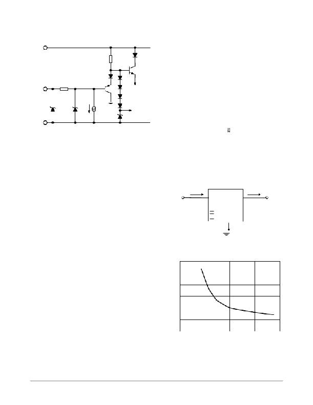
�Figure� 21.� NCV8501� Enable� Function� Equivalent�
�Circuit�
�Z1,� R1,� and� Z2� provide� ESD� and� overvoltage� protection.�
�Note� that,� for� ENABLE� pin� voltages� in� excess� of� 10� V,� an�
�external� series� resistor� is� required� to� limit� the� current� into�
�Z1.�
�For� ENABLE� pin� voltages� less� than� +7� V,� the� 5� m� A�
�(maximum� value)� current� source� dominates� the� input�
�current,� as� the� opposing� P1� base� current� is� negligible� by�
�(eq.� 2)�
�PD�
�The� value� of� R� q� JA� can� then� be� compared� with� those� in� the�
�package� section� of� the� data� sheet.� Those� packages� with�
�R� q� JA� ’s� less� than� the� calculated� value� in� Equation� 2� will� keep�
�the� die� temperature� below� 150� °� C.�
�In� some� cases,� none� of� the� packages� will� be� sufficient� to�
�dissipate� the� heat� generated� by� the� IC,� and� an� external�
�heatsink� will� be� required.�
�comparison.�
�For� ENABLE� pin� voltages� between� +7� V� and� +11� V,� the�
�input� current� is� given� by:�
�V� IN�
�I� IN�
�SMART�
�REGULATOR� ?�
�I� OUT�
�V� OUT�
�5� m� A� +� ((V� ENABLE� ?� 7)� /� 20� k� W� )�
�For� ENABLE� pin� voltages� in� excess� of� 10� V� (Z1�
�breakover� voltage� can� be� as� low� as� 10� V),� the� input� current�
�is� dominated� by� the� external� series� resistor.� For� the� case�
�where� V� ENABLE� =� 12� V;� R� EXT� =� 10� k� W� ,� the� input� current� can�
�be� up� to� (2� V/10� k� W� ),� =� 200� m� A.�
�The� ENABLE� threshold� is� that� voltage� required� to�
�achieve� ~3.85� V� at� the� base� of� N1,� or� approximately� (3.85� V�
�?� 2� Vbe).� At� +20� °� C,� this� threshold� is� ~2.55� V.� At� ?� 40� °� C,� it�
�can� be� as� high� as� 3� V.�
�If� the� value� of� R� EXT� is� increased� to� ~200� k� W� ,� to� reduce�
�ENABLE� input� current,� then� the� worst� ?� case� drop� across�
�R� EXT� must� be� added� to� 3� V� to� determine� the� effective�
�maximum� ENABLE� threshold.� At� V� ENABLE� <� 7� V,� we� only�
�need� to� consider� the� 5� m� A� current� sink.�
�Max� effective� threshold� =� 3� V� +� (5� m� A� *� 220� k� W� )�
�=� 3� V� +� 1.1� V�
�=� 4.1� V�
�Control�
�}� Features�
�I� Q�
�Figure� 22.� Single� Output� Regulator� with� Key�
�Performance� Parameters� Labeled�
�100�
�90�
�80�
�70�
�60�
�50�
�40�
�0�
�200�
�400�
�600�
�800�
�Copper� Area� (mm� 2� )�
�Figure� 23.� 16� Lead� SOW� (Exposed� Pad),� q� JA� as� a�
�Function� of� the� Pad� Copper� Area� (2� oz.� Cu�
�Thickness),� Board� Material� =� 0.0625� ,� G� ?� 10/R� ?� 4�
�http://onsemi.com�
�12�
�相关PDF资料 |
PDF描述 |
|---|---|
| LM4040A20IDBZR | IC VREF SHUNT PREC 2.048V SOT23 |
| AIML-1206-R22K-T | INDUCTOR MULTILAYER 0.22UH 1206 |
| ACC35DREI-S93 | CONN EDGECARD 70POS .100 EYELET |
| ABC35DREI-S93 | CONN EDGECARD 70POS .100 EYELET |
| MIC2845A-PPYMT TR | IC LED DRIVR WHITE BCKLGT 14TMLF |
相关代理商/技术参数 |
参数描述 |
|---|---|
| NCV8501D100R2 | 功能描述:低压差稳压器 - LDO 10V 150mA w/ENABLE RoHS:否 制造商:Texas Instruments 最大输入电压:36 V 输出电压:1.4 V to 20.5 V 回动电压(最大值):307 mV 输出电流:1 A 负载调节:0.3 % 输出端数量: 输出类型:Fixed 最大工作温度:+ 125 C 安装风格:SMD/SMT 封装 / 箱体:VQFN-20 |
| NCV8501D100R2G | 功能描述:低压差稳压器 - LDO 10V 150mA w/ENABLE RoHS:否 制造商:Texas Instruments 最大输入电压:36 V 输出电压:1.4 V to 20.5 V 回动电压(最大值):307 mV 输出电流:1 A 负载调节:0.3 % 输出端数量: 输出类型:Fixed 最大工作温度:+ 125 C 安装风格:SMD/SMT 封装 / 箱体:VQFN-20 |
| NCV8501D25 | 功能描述:低压差稳压器 - LDO 2.5V 150mA w/ENABLE RoHS:否 制造商:Texas Instruments 最大输入电压:36 V 输出电压:1.4 V to 20.5 V 回动电压(最大值):307 mV 输出电流:1 A 负载调节:0.3 % 输出端数量: 输出类型:Fixed 最大工作温度:+ 125 C 安装风格:SMD/SMT 封装 / 箱体:VQFN-20 |
| NCV8501D25G | 功能描述:低压差稳压器 - LDO 2.5V 150mA w/ENABLE RoHS:否 制造商:Texas Instruments 最大输入电压:36 V 输出电压:1.4 V to 20.5 V 回动电压(最大值):307 mV 输出电流:1 A 负载调节:0.3 % 输出端数量: 输出类型:Fixed 最大工作温度:+ 125 C 安装风格:SMD/SMT 封装 / 箱体:VQFN-20 |
| NCV8501D25R2 | 功能描述:低压差稳压器 - LDO 2.5V 150mA w/ENABLE RoHS:否 制造商:Texas Instruments 最大输入电压:36 V 输出电压:1.4 V to 20.5 V 回动电压(最大值):307 mV 输出电流:1 A 负载调节:0.3 % 输出端数量: 输出类型:Fixed 最大工作温度:+ 125 C 安装风格:SMD/SMT 封装 / 箱体:VQFN-20 |
发布紧急采购,3分钟左右您将得到回复。