- 您现在的位置:买卖IC网 > PDF目录19917 > NCV8502PDW100G (ON Semiconductor)IC REG LDO 10V .15A 16-SOIC PDF资料下载
参数资料
| 型号: | NCV8502PDW100G |
| 厂商: | ON Semiconductor |
| 文件页数: | 10/14页 |
| 文件大小: | 0K |
| 描述: | IC REG LDO 10V .15A 16-SOIC |
| 标准包装: | 47 |
| 稳压器拓扑结构: | 正,固定式 |
| 输出电压: | 10V |
| 输入电压: | 最高 45 V |
| 电压 - 压降(标准): | 0.4V @ 150mA |
| 稳压器数量: | 1 |
| 电流 - 输出: | 150mA |
| 电流 - 限制(最小): | 151mA |
| 工作温度: | -40°C ~ 150°C |
| 安装类型: | 表面贴装 |
| 封装/外壳: | 16-SOIC(0.295",7.50mm 宽)裸露焊盘 |
| 供应商设备封装: | 16-SOIC W |
| 包装: | 管件 |
�� �
�
�NCV8502� Series�
�APPLICATION� NOTES�
�V� IN�
�V� OUT�
�V� IN�
�NCV8502�
�V� OUT�
�V� ADJ�
�MJD31C�
�>1� Amp�
�5.0� V�
�C� IN� *�
�0.1� m� F�
�NCV8502�
�RESET�
�R� RST�
�C� OUT� **�
�10� m� F�
�V� BAT�
�C2�
�0.1� m� F�
�R1�
�294� k�
�R2�
�100� k�
�C1�
�47� m� F�
�*C� IN� required� if� regulator� is� located� far� from� the� power� supply� filter�
�**C� OUT� required� for� stability.� Capacitor� must� operate� at� minimum�
�temperature� expected�
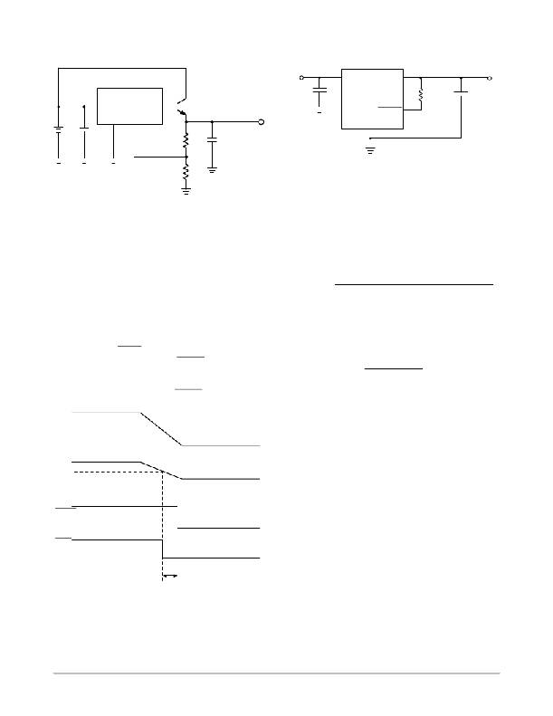
�Figure� 18.� Test� and� Application� Circuit� Showing�
�Output� Compensation�
�Figure� 16.� Additional� Output� Current�
�Adding� Capability�
�Figure� 16� shows� how� the� adjustable� version� of� parts� can�
�be� used� with� an� external� pass� transistor� for� additional� current�
�SETTING� THE� DELAY� TIME�
�The� delay� time� is� controlled� by� the� Reset� Delay� Low�
�Voltage,� Delay� Switching� Threshold,� and� the� Delay� Charge�
�Current.� The� delay� follows� the� equation:�
�capability.� The� setup� as� shown� will� provide� greater� than� 1�
�Amp� of� output� current.�
�tDELAY� +�
�CDELAY(Vdt� *� Reset Delay Low Voltage)�
�Delay� Charge� Current�
�FLAG� MONITOR�
�Figure� 17� shows� the� FLAG� Monitor� waveforms� as� a� result�
�of� the� circuit� depicted� in� Figure� 14.� As� the� output� voltage�
�falls� (V� OUT� ),� the� Monitor� threshold� is� crossed.� This� causes�
�the� voltage� on� the� FLAG� output� to� go� low� sending� a� warning�
�Example:�
�Using� C� DELAY� =� 33� nF.�
�Assume� reset� Delay� Low� Voltage� =� 0.�
�Use� the� typical� value� for� V� dt� =� 1.8� V.�
�Use� the� typical� value� for� Delay� Charge� Current� =� 2.5� m� A.�
�signal� to� the� microprocessor� that� a� RESET� signal� may� occur�
�in� a� short� period� of� time.� T� WARNING� is� the� time� the�
�microprocessor� has� to� complete� the� function� it� is� currently�
�tDELAY� +�
�33 nF(1.8� *� 0)�
�2.5� m� A�
�+� 23.8� ms�
�working� on� and� get� ready� for� the� RESET� shutdown� signal.�
�V� OUT�
�MON�
�FLAG� Monitor�
�Ref.� Voltage�
�STABILITY� CONSIDERATIONS�
�The� output� or� compensation� capacitor� helps� determine�
�three� main� characteristics� of� a� linear� regulator:� start� ?� up�
�delay,� load� transient� response� and� loop� stability.�
�The� capacitor� value� and� type� should� be� based� on� cost,�
�availability,� size� and� temperature� constraints.�
�The� value� for� the� output� capacitor� C� OUT� shown� in� Figure� 18�
�should� work� for� most� applications,� however� it� is� not�
�necessarily� the� optimized� solution.�
�RESET�
�FLAG�
�T� WARNING�
�Figure� 17.� FLAG� Monitor� Circuit� Waveform�
�http://onsemi.com�
�10�
�相关PDF资料 |
PDF描述 |
|---|---|
| GBB50DHBT | CONN EDGECARD 100PS R/A .050 SLD |
| LTC4251-2IS6#TRM | IC CTRLR HOTSWP NEG VOLT SOT23-6 |
| ACC22DRST-S273 | CONN EDGECARD 44POS DIP .100 SLD |
| RSM36DTKN-S288 | CONN EDGECARD 72POS .156 EXTEND |
| HBC07DRYS | CONN EDGECARD 14POS DIP .100 SLD |
相关代理商/技术参数 |
参数描述 |
|---|---|
| NCV8502PDW100R2 | 功能描述:低压差稳压器 - LDO 10V 150mA w/Delay RoHS:否 制造商:Texas Instruments 最大输入电压:36 V 输出电压:1.4 V to 20.5 V 回动电压(最大值):307 mV 输出电流:1 A 负载调节:0.3 % 输出端数量: 输出类型:Fixed 最大工作温度:+ 125 C 安装风格:SMD/SMT 封装 / 箱体:VQFN-20 |
| NCV8502PDW100R2G | 功能描述:低压差稳压器 - LDO 10V 150mA w/Delay RoHS:否 制造商:Texas Instruments 最大输入电压:36 V 输出电压:1.4 V to 20.5 V 回动电压(最大值):307 mV 输出电流:1 A 负载调节:0.3 % 输出端数量: 输出类型:Fixed 最大工作温度:+ 125 C 安装风格:SMD/SMT 封装 / 箱体:VQFN-20 |
| NCV8502PDW25 | 功能描述:低压差稳压器 - LDO 2.5V 150mA w/Delay RoHS:否 制造商:Texas Instruments 最大输入电压:36 V 输出电压:1.4 V to 20.5 V 回动电压(最大值):307 mV 输出电流:1 A 负载调节:0.3 % 输出端数量: 输出类型:Fixed 最大工作温度:+ 125 C 安装风格:SMD/SMT 封装 / 箱体:VQFN-20 |
| NCV8502PDW25G | 功能描述:低压差稳压器 - LDO 2.5V 150mA w/Delay RoHS:否 制造商:Texas Instruments 最大输入电压:36 V 输出电压:1.4 V to 20.5 V 回动电压(最大值):307 mV 输出电流:1 A 负载调节:0.3 % 输出端数量: 输出类型:Fixed 最大工作温度:+ 125 C 安装风格:SMD/SMT 封装 / 箱体:VQFN-20 |
| NCV8502PDW25R2 | 功能描述:低压差稳压器 - LDO 2.5V 150mA w/Delay RoHS:否 制造商:Texas Instruments 最大输入电压:36 V 输出电压:1.4 V to 20.5 V 回动电压(最大值):307 mV 输出电流:1 A 负载调节:0.3 % 输出端数量: 输出类型:Fixed 最大工作温度:+ 125 C 安装风格:SMD/SMT 封装 / 箱体:VQFN-20 |
发布紧急采购,3分钟左右您将得到回复。