- 您现在的位置:买卖IC网 > PDF目录299551 > NCV8503PDW25 (ON SEMICONDUCTOR) 2.5 V FIXED POSITIVE LDO REGULATOR, PDSO16 PDF资料下载
参数资料
| 型号: | NCV8503PDW25 |
| 厂商: | ON SEMICONDUCTOR |
| 元件分类: | 固定正电压单路输出LDO稳压器 |
| 英文描述: | 2.5 V FIXED POSITIVE LDO REGULATOR, PDSO16 |
| 封装: | EXPOSED PAD, SOW-16 |
| 文件页数: | 11/12页 |
| 文件大小: | 89K |
| 代理商: | NCV8503PDW25 |
NCV8503 Series
http://onsemi.com
8
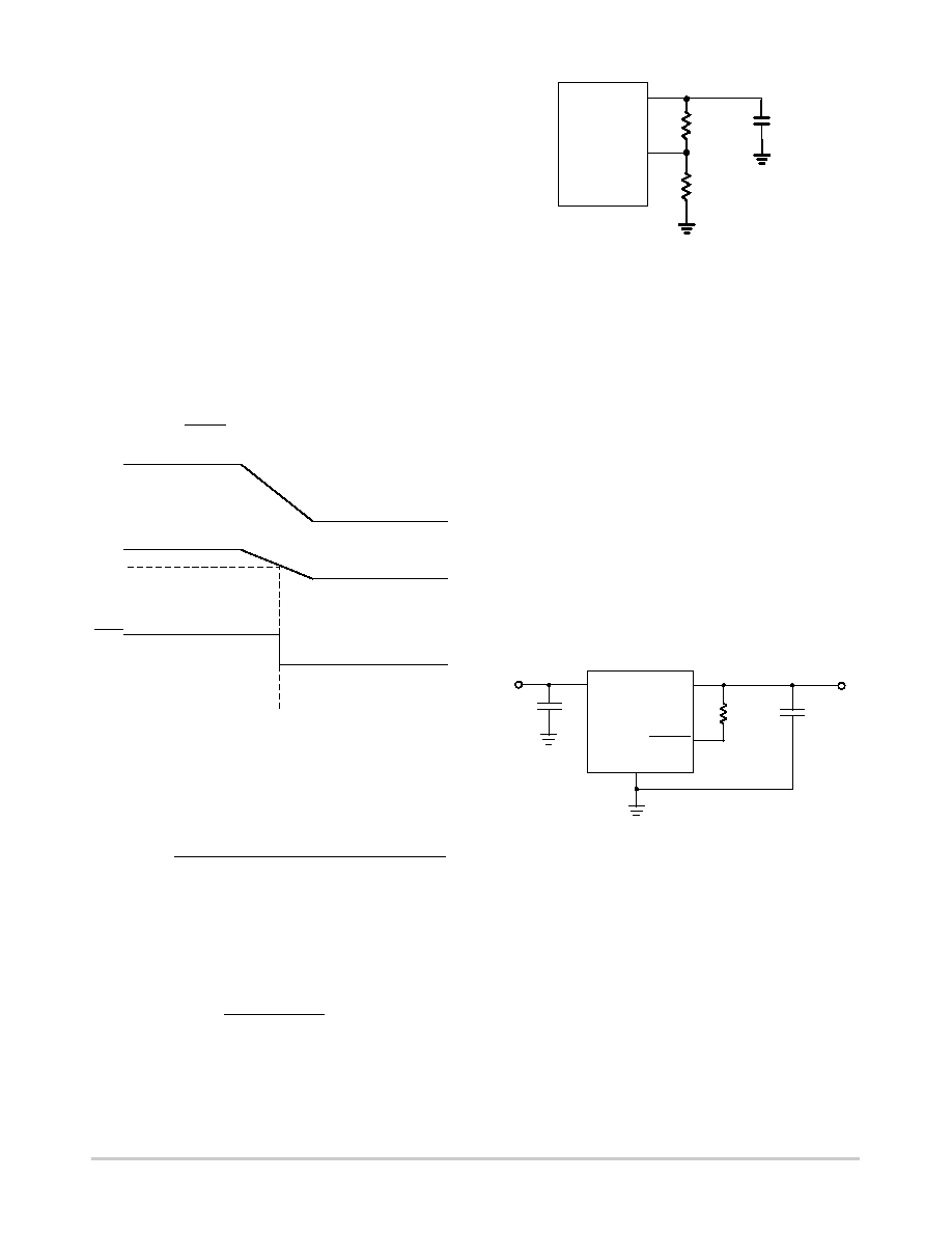
Voltage Adjust
Figure 7 shows the device setup for a user configurable
output voltage. The feedback to the VADJ pin is taken from
a voltage divider referenced to the output voltage. The loop
is balanced around the Unity Gain threshold (1.30 V
typical).
Figure 7. Adjustable Output Voltage
VOUT
VADJ
NCV8503
15 k
5.1 k
COUT
≈5.0 V
1.28 V
APPLICATION NOTES
FLAG MONITOR
Figure 8 shows the FLAG Monitor waveforms as a result
of the circuit depicted in Figure 6. As the input voltage falls
(VMON), the Monitor threshold is crossed. This causes the
voltage on the FLAG output to go low.
Figure 8. FLAG Monitor Circuit Waveform
VMON
MON
Flag Monitor
Ref. Voltage
FLAG
SETTING THE DELAY TIME
The delay time is controlled by the Reset Delay Low
Voltage, Delay Switching Threshold, and the Delay Charge
Current. The delay follows the equation:
tDELAY +
[CDELAY(Vdt * Reset Delay Low Voltage)]
Delay Charge Current
Example:
Using CDELAY = 33 nF.
Assume reset Delay Low Voltage = 0.
Use the typical value for Vdt = 1.8 V (2.5 V, 3.3 V, and
5.0 V options).
Use the typical value for Delay Charge Current = 4.2
A.
tDELAY +
[33 nF(1.8
* 0)]
4.2
mA
+ 14 ms
STABILITY CONSIDERATIONS
The output or compensation capacitor helps determine
three main characteristics of a linear regulator: startup
delay, load transient response and loop stability.
The capacitor value and type should be based on cost,
availability, size and temperature constraints. A tantalum or
aluminum electrolytic capacitor is best, since a film or
ceramic capacitor with almost zero ESR can cause
instability. The aluminum electrolytic capacitor is the least
expensive solution, but, if the circuit operates at low
temperatures (25
°C to 40°C), both the value and ESR of
the capacitor will vary considerably. The capacitor
manufacturers data sheet usually provides this information.
The value for the output capacitor COUT shown in Figure 9
should work for most applications, however it is not
necessarily the optimized solution.
Figure 9. Test and Application Circuit Showing
Output Compensation
VIN
VOUT
COUT**
33
F
RRST
RESET
CIN*
0.1
F
NCV8503
*CIN required if regulator is located far from the power supply filter
**COUT required for stability. Capacitor must operate at minimum
temperature expected
相关PDF资料 |
PDF描述 |
|---|---|
| NCV8503PDW33R2 | 3.3 V FIXED POSITIVE LDO REGULATOR, PDSO16 |
| NCV8503PDW33 | 3.3 V FIXED POSITIVE LDO REGULATOR, PDSO16 |
| ND2012L-2-18 | 160 mA, 200 V, N-CHANNEL, Si, SMALL SIGNAL, MOSFET, TO-226AA |
| NDB6030L/S62Z | 52 A, 30 V, 0.0135 ohm, N-CHANNEL, Si, POWER, MOSFET, TO-263AB |
| NDB7052/L86Z | 75 A, 50 V, 0.01 ohm, N-CHANNEL, Si, POWER, MOSFET, TO-263AB |
相关代理商/技术参数 |
参数描述 |
|---|---|
| NCV8503PW25 | 功能描述:低压差稳压器 - LDO 2.5V 400mA w/ENABLE RoHS:否 制造商:Texas Instruments 最大输入电压:36 V 输出电压:1.4 V to 20.5 V 回动电压(最大值):307 mV 输出电流:1 A 负载调节:0.3 % 输出端数量: 输出类型:Fixed 最大工作温度:+ 125 C 安装风格:SMD/SMT 封装 / 箱体:VQFN-20 |
| NCV8503PW25G | 功能描述:低压差稳压器 - LDO 2.5V 400mA w/ENABLE RoHS:否 制造商:Texas Instruments 最大输入电压:36 V 输出电压:1.4 V to 20.5 V 回动电压(最大值):307 mV 输出电流:1 A 负载调节:0.3 % 输出端数量: 输出类型:Fixed 最大工作温度:+ 125 C 安装风格:SMD/SMT 封装 / 箱体:VQFN-20 |
| NCV8503PW25R2 | 功能描述:低压差稳压器 - LDO 2.5V 400mA w/ENABLE RoHS:否 制造商:Texas Instruments 最大输入电压:36 V 输出电压:1.4 V to 20.5 V 回动电压(最大值):307 mV 输出电流:1 A 负载调节:0.3 % 输出端数量: 输出类型:Fixed 最大工作温度:+ 125 C 安装风格:SMD/SMT 封装 / 箱体:VQFN-20 |
| NCV8503PW25R2G | 功能描述:低压差稳压器 - LDO 2.5V 400mA w/ENABLE RoHS:否 制造商:Texas Instruments 最大输入电压:36 V 输出电压:1.4 V to 20.5 V 回动电压(最大值):307 mV 输出电流:1 A 负载调节:0.3 % 输出端数量: 输出类型:Fixed 最大工作温度:+ 125 C 安装风格:SMD/SMT 封装 / 箱体:VQFN-20 |
| NCV8503PW33 | 功能描述:低压差稳压器 - LDO 3.3V 400mA w/ENABLE RoHS:否 制造商:Texas Instruments 最大输入电压:36 V 输出电压:1.4 V to 20.5 V 回动电压(最大值):307 mV 输出电流:1 A 负载调节:0.3 % 输出端数量: 输出类型:Fixed 最大工作温度:+ 125 C 安装风格:SMD/SMT 封装 / 箱体:VQFN-20 |
发布紧急采购,3分钟左右您将得到回复。