- 您现在的位置:买卖IC网 > PDF目录19903 > NCV8503PW33G (ON Semiconductor)IC REG LDO 3.3V .4A 16-SOIC PDF资料下载
参数资料
| 型号: | NCV8503PW33G |
| 厂商: | ON Semiconductor |
| 文件页数: | 11/13页 |
| 文件大小: | 0K |
| 描述: | IC REG LDO 3.3V .4A 16-SOIC |
| 标准包装: | 47 |
| 稳压器拓扑结构: | 正,固定式 |
| 输出电压: | 3.3V |
| 输入电压: | 最高 45 V |
| 稳压器数量: | 1 |
| 电流 - 输出: | 400mA |
| 电流 - 限制(最小): | 425mA |
| 工作温度: | -40°C ~ 150°C |
| 安装类型: | 表面贴装 |
| 封装/外壳: | 16-SOIC(0.295",7.50mm 宽)裸露焊盘 |
| 供应商设备封装: | 16-SOIC W |
| 包装: | 管件 |
�� �
�
�NCV8503� Series�
�100�
�90�
�80�
�70�
�The� value� of� R� q� JA� can� then� be� compared� with� those� in� the�
�package� section� of� the� data� sheet.� Those� packages� with�
�R� q� JA� ’s� less� than� the� calculated� value� in� equation� 2� will� keep�
�the� die� temperature� below� 150� °� C.�
�In� some� cases,� none� of� the� packages� will� be� sufficient� to�
�dissipate� the� heat� generated� by� the� IC,� and� an� external�
�heatsink� will� be� required.�
�60�
�I� IN�
�I� OUT�
�50�
�V� IN�
�SMART�
�REGULATOR� ?�
�V� OUT�
�T�
�R� q� JA� +� 150� C� *� A�
�PD�
�R� q� JA� +� R� q� JC� )� R� q� CS� )� R� q� SA�
�40�
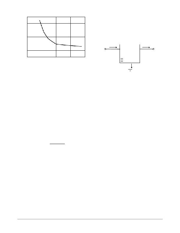
�0� 200� 400� 600� 800�
�Copper� Area� (mm� 2� )�
�Figure� 22.� 16� Lead� SOW� (Exposed� Pad),� q� JA� as� a�
�Function� of� the� Pad� Copper� Area� (2� oz.� Cu�
�Thickness),� Board� Material� =� 0.0625� ,� G� ?� 10/R� ?� 4�
�CALCULATING� POWER� DISSIPATION� IN� A�
�SINGLE� OUTPUT� LINEAR� REGULATOR�
�The� maximum� power� dissipation� for� a� single� output�
�regulator� (Figure� 23)� is:�
�PD(max)� +� [VIN(max)� *� VOUT(min)]� IOUT(max)� (1)�
�)� VIN(max)IQ�
�where:�
�V� IN(max)� is� the� maximum� input� voltage,�
�V� OUT(min)� is� the� minimum� output� voltage,�
�I� OUT(max)� is� the� maximum� output� current� for� the�
�application,� and�
�I� Q� is� the� quiescent� current� the� regulator� consumes� at�
�I� OUT(max)� .�
�Once� the� value� of� P� D(max)� is� known,� the� maximum�
�permissible� value� of� R� q� JA� can� be� calculated:�
�o�
�(2)�
�Control�
�}� Features�
�I� Q�
�Figure� 23.� Single� Output� Regulator� with� Key�
�Performance� Parameters� Labeled�
�HEAT� SINKS�
�A� heat� sink� effectively� increases� the� surface� area� of� the�
�package� to� improve� the� flow� of� heat� away� from� the� IC� and�
�into� the� surrounding� air.�
�Each� material� in� the� heat� flow� path� between� the� IC� and� the�
�outside� environment� will� have� a� thermal� resistance.� Like�
�series� electrical� resistances,� these� resistances� are� summed� to�
�determine� the� value� of� R� q� JA� :�
�(3)�
�where:�
�R� q� JC� =� the� junction� ?� to� ?� case� thermal� resistance,�
�R� q� CS� =� the� case� ?� to� ?� heatsink� thermal� resistance,� and�
�R� q� SA� =� the� heatsink� ?� to� ?� ambient� thermal� resistance.�
�R� q� JC� appears� in� the� package� section� of� the� data� sheet.� Like�
�R� q� JA� ,� it� too� is� a� function� of� package� type.� R� q� CS� and� R� q� SA� are�
�functions� of� the� package� type,� heatsink� and� the� interface�
�between� them.� These� values� appear� in� heat� sink� data� sheets�
�of� heat� sink� manufacturers.�
�http://onsemi.com�
�11�
�相关PDF资料 |
PDF描述 |
|---|---|
| 1235F10 | BATTERY PK S-HD 15.0V CSIZE ZINC |
| VY2222M35Y5US6UL7 | CAP CER 2200PF 300V 20% RADIAL |
| LT4250HCS8#TR | IC CONTRLR HOTSWAP NEG 48V 8SOIC |
| NCV8503PW25G | IC REG LDO 2.5V .4A 16-SOIC |
| T95R226K050EABS | CAP TANT 22UF 50V 10% 2824 |
相关代理商/技术参数 |
参数描述 |
|---|---|
| NCV8503PW33R2 | 功能描述:低压差稳压器 - LDO 3.3V 400mA w/ENABLE RoHS:否 制造商:Texas Instruments 最大输入电压:36 V 输出电压:1.4 V to 20.5 V 回动电压(最大值):307 mV 输出电流:1 A 负载调节:0.3 % 输出端数量: 输出类型:Fixed 最大工作温度:+ 125 C 安装风格:SMD/SMT 封装 / 箱体:VQFN-20 |
| NCV8503PW33R2G | 功能描述:低压差稳压器 - LDO 3.3V 400mA w/ENABLE RoHS:否 制造商:Texas Instruments 最大输入电压:36 V 输出电压:1.4 V to 20.5 V 回动电压(最大值):307 mV 输出电流:1 A 负载调节:0.3 % 输出端数量: 输出类型:Fixed 最大工作温度:+ 125 C 安装风格:SMD/SMT 封装 / 箱体:VQFN-20 |
| NCV8503PW50 | 功能描述:低压差稳压器 - LDO 5.0V 400mA w/ENABLE RoHS:否 制造商:Texas Instruments 最大输入电压:36 V 输出电压:1.4 V to 20.5 V 回动电压(最大值):307 mV 输出电流:1 A 负载调节:0.3 % 输出端数量: 输出类型:Fixed 最大工作温度:+ 125 C 安装风格:SMD/SMT 封装 / 箱体:VQFN-20 |
| NCV8503PW50G | 功能描述:低压差稳压器 - LDO 5.0V 400mA w/ENABLE RoHS:否 制造商:Texas Instruments 最大输入电压:36 V 输出电压:1.4 V to 20.5 V 回动电压(最大值):307 mV 输出电流:1 A 负载调节:0.3 % 输出端数量: 输出类型:Fixed 最大工作温度:+ 125 C 安装风格:SMD/SMT 封装 / 箱体:VQFN-20 |
| NCV8503PW50R2 | 功能描述:低压差稳压器 - LDO 5.0V 400mA w/ENABLE RoHS:否 制造商:Texas Instruments 最大输入电压:36 V 输出电压:1.4 V to 20.5 V 回动电压(最大值):307 mV 输出电流:1 A 负载调节:0.3 % 输出端数量: 输出类型:Fixed 最大工作温度:+ 125 C 安装风格:SMD/SMT 封装 / 箱体:VQFN-20 |
发布紧急采购,3分钟左右您将得到回复。