- 您现在的位置:买卖IC网 > PDF目录19216 > NCV8505D2T33G (ON Semiconductor)IC REG LDO 3.3V .4A D2PAK-7 PDF资料下载
参数资料
| 型号: | NCV8505D2T33G |
| 厂商: | ON Semiconductor |
| 文件页数: | 9/12页 |
| 文件大小: | 0K |
| 描述: | IC REG LDO 3.3V .4A D2PAK-7 |
| 产品变化通告: | 1Q2012 Discontinuation 30/Mar/2012 |
| 标准包装: | 50 |
| 稳压器拓扑结构: | 正,固定式 |
| 输出电压: | 3.3V |
| 输入电压: | 最高 45 V |
| 稳压器数量: | 1 |
| 电流 - 输出: | 400mA |
| 电流 - 限制(最小): | 425mA |
| 工作温度: | -40°C ~ 150°C |
| 安装类型: | 表面贴装 |
| 封装/外壳: | TO-263-8,D²Pak(7 引线+接片),TO-263CA |
| 供应商设备封装: | D2PAK-7 |
| 包装: | 管件 |
�� �
�
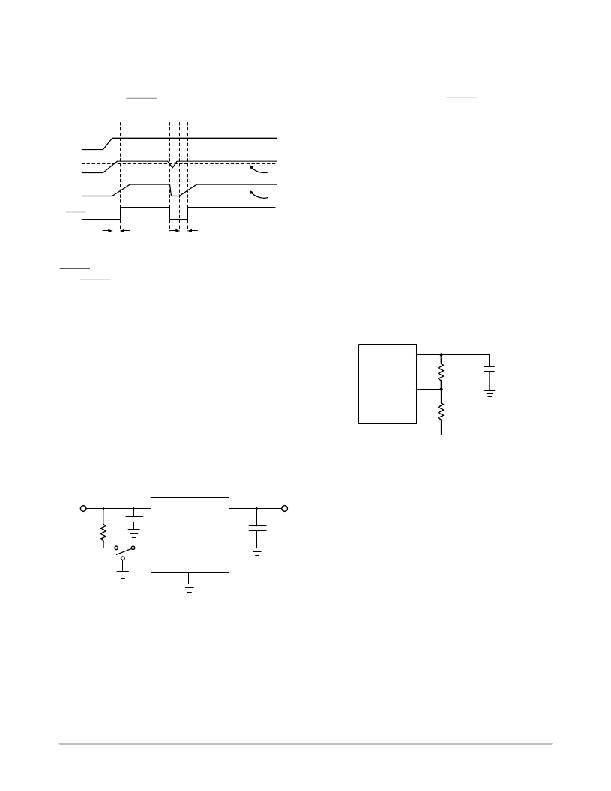
�NCV8505� Series�
�CIRCUIT� DESCRIPTION�
�REGULATOR� CONTROL� FUNCTIONS�
�The� NCV8505� contains� the� microprocessor� compatible�
�control� function� RESET� (Figure� 15).�
�V� IN�
�DELAY� Function�
�The� reset� delay� circuit� provides� a� programmable� (by�
�external� capacitor)� delay� on� the� RESET� output� lead.�
�The� DELAY� lead� provides� source� current� (typically� 4.0� m� A)�
�to� the� external� DELAY� capacitor� during� the� following�
�proceedings:�
�1.� During� Power� Up� (once� the� regulation� threshold�
�V� OUT�
�DELAY�
�RESET�
�RESET�
�Threshold�
�DELAY�
�Threshold�
�(V� DT� )�
�has� been� verified).�
�2.� After� a� reset� event� has� occurred� and� the� device� is�
�back� in� regulation.� The� DELAY� capacitor� is�
�discharged� when� the� regulation� (RESET� threshold)�
�has� been� violated.� This� is� a� latched� incident.� The�
�capacitor� will� fully� discharge� and� wait� for� the�
�T� d� T� d�
�Figure� 15.� Reset� and� Delay� Circuit� Wave� Forms�
�RESET� Function�
�A� RESET� signal� (low� voltage)� is� generated� as� the� IC�
�powers� up� until� V� OUT� is� within� 1.5%� of� the� regulated� output�
�voltage,� or� when� V� OUT� drops� out� of� regulation,and� is� lower�
�than� 4.0%� below� the� regulated� output� voltage.� Hysteresis� is�
�included� in� the� function� to� minimize� oscillations.�
�device� to� regulate� before� going� through� the� delay�
�time� event� again.�
�Voltage� Adjust�
�Figure� 17� shows� the� device� setup� for� a� user� configurable�
�output� voltage.� The� feedback� to� the� V� ADJ� pin� is� taken� from�
�a� voltage� divider� referenced� to� the� output� voltage.� The� loop�
�is� balanced� around� the� Unity� Gain� threshold� (1.30� V�
�typical).�
�The� RESET� output� is� an� open� collector� NPN� transistor,�
�controlled� by� a� low� voltage� detection� circuit.� The� circuit� is�
�V� OUT�
�≈� 5.0� V�
�functionally� independent� of� the� rest� of� the� IC� thereby�
�guaranteeing� that� the� RESET� signal� is� valid� for� V� OUT� as� low�
�as� 1.0� V.�
�ENABLE� Function�
�NCV8505�
�V� ADJ�
�15� k�
�1.28� V�
�5.1� k�
�C� OUT�
�The� part� stays� in� a� low� I� Q� sleep� mode� when� the� ENABLE�
�pin� is� held� low.� The� part� has� an� internal� pull� down� if� the� pin�
�is� left� floating.�
�The� integrity� of� the� ENABLE� pin� allows� it� to� be� tied� to� the�
�battery� line� through� an� external� resistor.� It� will� withstand�
�load� dump� potentials� in� this� configuration.�
�Figure� 17.� Adjustable� Output� Voltage�
�V� BAT�
�Up� to� 45� V�
�10� k�
�V� IN�
�NCV8505�
�V� OUT�
�ENABLE�
�GND�
�Figure� 16.� ENABLE� Function�
�http://onsemi.com�
�9�
�相关PDF资料 |
PDF描述 |
|---|---|
| NCV8505D2T33 | IC REG LDO 3.3V .4A D2PAK-7 |
| VE-B4B-CW-S | CONVERTER MOD DC/DC 95V 100W |
| TAJV686M035RNJ | CAP TANT 68UF 35V 20% 2924 |
| TH3B226K6R3D1500 | CAP TANT 22UF 6.3V 10% 1411 |
| VE-B44-CW-S | CONVERTER MOD DC/DC 48V 100W |
相关代理商/技术参数 |
参数描述 |
|---|---|
| NCV8505D2T33R4 | 功能描述:低压差稳压器 - LDO 3.3V 400mA w/ENABLE RoHS:否 制造商:Texas Instruments 最大输入电压:36 V 输出电压:1.4 V to 20.5 V 回动电压(最大值):307 mV 输出电流:1 A 负载调节:0.3 % 输出端数量: 输出类型:Fixed 最大工作温度:+ 125 C 安装风格:SMD/SMT 封装 / 箱体:VQFN-20 |
| NCV8505D2T33R4G | 功能描述:低压差稳压器 - LDO MICROPOWER 400 RoHS:否 制造商:Texas Instruments 最大输入电压:36 V 输出电压:1.4 V to 20.5 V 回动电压(最大值):307 mV 输出电流:1 A 负载调节:0.3 % 输出端数量: 输出类型:Fixed 最大工作温度:+ 125 C 安装风格:SMD/SMT 封装 / 箱体:VQFN-20 |
| NCV8505D2T50 | 功能描述:低压差稳压器 - LDO 5.0V 400mA w/ENABLE RoHS:否 制造商:Texas Instruments 最大输入电压:36 V 输出电压:1.4 V to 20.5 V 回动电压(最大值):307 mV 输出电流:1 A 负载调节:0.3 % 输出端数量: 输出类型:Fixed 最大工作温度:+ 125 C 安装风格:SMD/SMT 封装 / 箱体:VQFN-20 |
| NCV8505D2T50G | 功能描述:低压差稳压器 - LDO 5.0V 400mA w/ENABLE RoHS:否 制造商:Texas Instruments 最大输入电压:36 V 输出电压:1.4 V to 20.5 V 回动电压(最大值):307 mV 输出电流:1 A 负载调节:0.3 % 输出端数量: 输出类型:Fixed 最大工作温度:+ 125 C 安装风格:SMD/SMT 封装 / 箱体:VQFN-20 |
| NCV8505D2T50R4 | 功能描述:低压差稳压器 - LDO 5.0V 400mA w/ENABLE RoHS:否 制造商:Texas Instruments 最大输入电压:36 V 输出电压:1.4 V to 20.5 V 回动电压(最大值):307 mV 输出电流:1 A 负载调节:0.3 % 输出端数量: 输出类型:Fixed 最大工作温度:+ 125 C 安装风格:SMD/SMT 封装 / 箱体:VQFN-20 |
发布紧急采购,3分钟左右您将得到回复。