- 您现在的位置:买卖IC网 > PDF目录19298 > NCV8505D2T50R4 (ON Semiconductor)IC REG LDO 5V .4A D2PAK7 PDF资料下载
参数资料
| 型号: | NCV8505D2T50R4 |
| 厂商: | ON Semiconductor |
| 文件页数: | 10/12页 |
| 文件大小: | 0K |
| 描述: | IC REG LDO 5V .4A D2PAK7 |
| 产品变化通告: | LTB Notification 03/Jan/2008 |
| 标准包装: | 750 |
| 稳压器拓扑结构: | 正,固定式 |
| 输出电压: | 5V |
| 输入电压: | 最高 45 V |
| 电压 - 压降(标准): | 0.4V @ 400mA |
| 稳压器数量: | 1 |
| 电流 - 输出: | 400mA |
| 电流 - 限制(最小): | 425mA |
| 工作温度: | -40°C ~ 150°C |
| 安装类型: | 表面贴装 |
| 封装/外壳: | TO-263-8,D²Pak(7 引线+接片),TO-263CA |
| 供应商设备封装: | D2PAK-7 |
| 包装: | 带卷 (TR) |
| 其它名称: | NCV8505D2T50R4OS |
�� �
�
�NCV8505� Series�
�APPLICATION� NOTES�
�tDELAY� +�
�tDELAY� +� +� 14� ms�
�T�
�R� q� JA� +� 150� C� *� A�
�PD�
�SETTING� THE� DELAY� TIME�
�The� delay� time� is� controlled� by� the� Reset� Delay� Low�
�Voltage,� Delay� Switching� Threshold,� and� the� Delay� Charge�
�Current.� The� delay� follows� the� equation:�
�CDELAY(Vdt� *� Reset Delay Low Voltage)�
�Delay� Charge� Current�
�Example:�
�Using� C� DELAY� =� 33� nF.�
�Assume� reset� Delay� Low� Voltage� =� 0.�
�Use� the� typical� value� for� V� dt� =� 1.8� V� (2.5� V,� 3.3� V,� and�
�5.0� V� options).�
�Use� the� typical� value� for� Delay� Charge� Current� =� 4.2� m� A.�
�33 nF(1.8� *� 0)�
�4.2� m� A�
�STABILITY� CONSIDERATIONS�
�The� output� or� compensation� capacitor� helps� determine�
�three� main� characteristics� of� a� linear� regulator:� start� ?� up�
�delay,� load� transient� response� and� loop� stability.�
�The� capacitor� value� and� type� should� be� based� on� cost,�
�PD(max)� +� [VIN(max)� *� VOUT(min)]� IOUT(max)� (1)�
�)� VIN(max)IQ�
�where:�
�V� IN(max)� is� the� maximum� input� voltage,�
�V� OUT(min)� is� the� minimum� output� voltage,�
�I� OUT(max)� is� the� maximum� output� current� for� the�
�application,� and�
�I� Q� is� the� quiescent� current� the� regulator� consumes� at�
�I� OUT(max)� .�
�Once� the� value� of� P� D(max)� is� known,� the� maximum�
�permissible� value� of� R� q� JA� can� be� calculated:�
�o�
�(2)�
�The� value� of� R� q� JA� can� then� be� compared� with� those� in� the�
�package� section� of� the� data� sheet.� Those� packages� with�
�R� q� JA� ’s� less� than� the� calculated� value� in� equation� 2� will� keep�
�the� die� temperature� below� 150� °� C.�
�In� some� cases,� none� of� the� packages� will� be� sufficient� to�
�dissipate� the� heat� generated� by� the� IC,� and� an� external�
�heatsink� will� be� required.�
�availability,� size� and� temperature� constraints.� A� tantalum� or�
�aluminum� electrolytic� capacitor� is� best,� since� a� film� or�
�ceramic� capacitor� with� almost� zero� ESR� can� cause�
�instability.� The� aluminum� electrolytic� capacitor� is� the� least�
�V� IN�
�I� IN�
�SMART�
�REGULATOR� ?�
�I� OUT�
�V� OUT�
�expensive� solution,� but,� if� the� circuit� operates� at� low�
�temperatures� (� ?� 25� °� C� to� ?� 40� °� C),� both� the� value� and� ESR� of�
�the� capacitor� will� vary� considerably.� The� capacitor�
�manufacturers� data� sheet� usually� provides� this� information.�
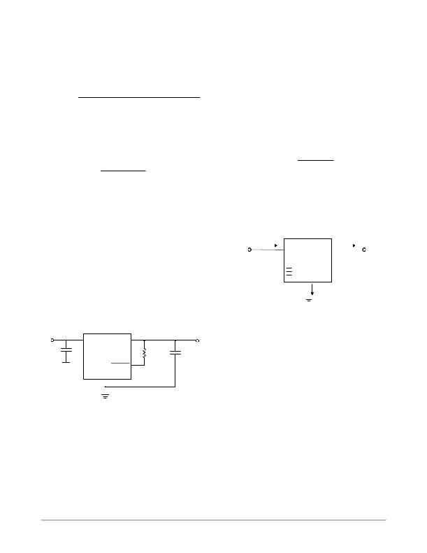
�The� value� for� the� output� capacitor� C� OUT� shown� in� Figure� 18�
�should� work� for� most� applications,� however� it� is� not�
�necessarily� the� optimized� solution.�
�Control�
�}� Features�
�I� Q�
�Figure� 19.� Single� Output� Regulator� with� Key�
�Performance� Parameters� Labeled�
�V� IN�
�V� OUT�
�HEAT� SINKS�
�A� heat� sink� effectively� increases� the� surface� area� of� the�
�C� IN� *�
�0.1� m� F�
�NCV8505�
�RESET�
�R� RST�
�C� OUT� **�
�33� m� F�
�package� to� improve� the� flow� of� heat� away� from� the� IC� and�
�into� the� surrounding� air.�
�Each� material� in� the� heat� flow� path� between� the� IC� and� the�
�outside� environment� will� have� a� thermal� resistance.� Like�
�series� electrical� resistances,� these� resistances� are� summed� to�
�determine� the� value� of� R� q� JA� :�
�R� q� JA� +� R� q� JC� )� R� q� CS� )� R� q� SA�
�*C� IN� required� if� regulator� is� located� far� from� the� power� supply�
�filter.�
�**C� OUT� required� for� stability.� Capacitor� must� operate� at� minimum�
�temperature� expected.�
�Figure� 18.� Test� and� Application� Circuit� Showing�
�Output� Compensation�
�CALCULATING� POWER� DISSIPATION� IN� A�
�SINGLE� OUTPUT� LINEAR� REGULATOR�
�The� maximum� power� dissipation� for� a� single� output�
�regulator� (Figure� 19)� is:�
�(3)�
�where:�
�R� q� JC� =� the� junction� ?� to� ?� case� thermal� resistance,�
�R� q� CS� =� the� case� ?� to� ?� heatsink� thermal� resistance,� and�
�R� q� SA� =� the� heatsink� ?� to� ?� ambient� thermal� resistance.�
�R� q� JC� appears� in� the� package� section� of� the� data� sheet.� Like�
�R� q� JA� ,� it� too� is� a� function� of� package� type.� R� q� CS� and� R� q� SA� are�
�functions� of� the� package� type,� heatsink� and� the� interface�
�between� them.� These� values� appear� in� heat� sink� data� sheets�
�of� heat� sink� manufacturers.�
�http://onsemi.com�
�10�
�相关PDF资料 |
PDF描述 |
|---|---|
| VI-21H-CW-F2 | CONVERTER MOD DC/DC 52V 100W |
| NCV8505D2TADJR4 | IC REG LDO ADJ .4A D2PAK-7 |
| GEC12DRTS | CONN EDGECARD 24POS DIP .100 SLD |
| F920G685MPA | CAP TANT 6.8UF 4V 20% 0805 |
| XC6VLX240T-1FFG784I | IC FPGA VIRTEX 6 241K 784FFGBGA |
相关代理商/技术参数 |
参数描述 |
|---|---|
| NCV8505D2T50R4G | 功能描述:低压差稳压器 - LDO 5.0V 400mA w/ENABLE RoHS:否 制造商:Texas Instruments 最大输入电压:36 V 输出电压:1.4 V to 20.5 V 回动电压(最大值):307 mV 输出电流:1 A 负载调节:0.3 % 输出端数量: 输出类型:Fixed 最大工作温度:+ 125 C 安装风格:SMD/SMT 封装 / 箱体:VQFN-20 |
| NCV8505D2TADJ | 功能描述:低压差稳压器 - LDO 400mA ADJ w/ENABLE RoHS:否 制造商:Texas Instruments 最大输入电压:36 V 输出电压:1.4 V to 20.5 V 回动电压(最大值):307 mV 输出电流:1 A 负载调节:0.3 % 输出端数量: 输出类型:Fixed 最大工作温度:+ 125 C 安装风格:SMD/SMT 封装 / 箱体:VQFN-20 |
| NCV8505D2TADJG | 功能描述:低压差稳压器 - LDO MICROPOWER 400 RoHS:否 制造商:Texas Instruments 最大输入电压:36 V 输出电压:1.4 V to 20.5 V 回动电压(最大值):307 mV 输出电流:1 A 负载调节:0.3 % 输出端数量: 输出类型:Fixed 最大工作温度:+ 125 C 安装风格:SMD/SMT 封装 / 箱体:VQFN-20 |
| NCV8505D2TADJR4 | 功能描述:低压差稳压器 - LDO 400mA ADJ w/ENABLE RoHS:否 制造商:Texas Instruments 最大输入电压:36 V 输出电压:1.4 V to 20.5 V 回动电压(最大值):307 mV 输出电流:1 A 负载调节:0.3 % 输出端数量: 输出类型:Fixed 最大工作温度:+ 125 C 安装风格:SMD/SMT 封装 / 箱体:VQFN-20 |
| NCV8505D2TADJR4G | 功能描述:低压差稳压器 - LDO MICROPOWER 400 RoHS:否 制造商:Texas Instruments 最大输入电压:36 V 输出电压:1.4 V to 20.5 V 回动电压(最大值):307 mV 输出电流:1 A 负载调节:0.3 % 输出端数量: 输出类型:Fixed 最大工作温度:+ 125 C 安装风格:SMD/SMT 封装 / 箱体:VQFN-20 |
发布紧急采购,3分钟左右您将得到回复。