- 您现在的位置:买卖IC网 > PDF目录19900 > NCV8506D2TADJG (ON Semiconductor)IC REG LDO ADJ .4A D2PAK-7 PDF资料下载
参数资料
| 型号: | NCV8506D2TADJG |
| 厂商: | ON Semiconductor |
| 文件页数: | 9/12页 |
| 文件大小: | 0K |
| 描述: | IC REG LDO ADJ .4A D2PAK-7 |
| 标准包装: | 50 |
| 稳压器拓扑结构: | 正,可调式 |
| 输出电压: | 可调 |
| 输入电压: | 最高 45 V |
| 电压 - 压降(标准): | 0.4V @ 400mA |
| 稳压器数量: | 1 |
| 电流 - 输出: | 400mA |
| 电流 - 限制(最小): | 425mA |
| 工作温度: | -40°C ~ 150°C |
| 安装类型: | 表面贴装 |
| 封装/外壳: | TO-263-8,D²Pak(7 引线+接片),TO-263CA |
| 供应商设备封装: | D2PAK-7 |
| 包装: | 管件 |
�� �
�
�NCV8506� Series�
�CIRCUIT� DESCRIPTION�
�REGULATOR� CONTROL� FUNCTIONS�
�The� NCV8506� contains� the� microprocessor� compatible�
�control� function� RESET� (Figure� 13).�
�V� IN�
�The� DELAY� lead� provides� source� current� (typically� 4.0� m� A)�
�to� the� external� DELAY� capacitor� during� the� following�
�proceedings:�
�1.� During� Power� Up� (once� the� regulation� threshold�
�has� been� verified).�
�2.� After� a� reset� event� has� occurred� and� the� device� is�
�back� in� regulation.� The� DELAY� capacitor� is�
�V� OUT�
�DELAY�
�RESET�
�RESET�
�Threshold�
�DELAY�
�Threshold�
�(V� DT� )�
�discharged� when� the� regulation� (RESET� threshold)�
�has� been� violated.� This� is� a� latched� incident.� The�
�capacitor� will� fully� discharge� and� wait� for� the�
�device� to� regulate� before� going� through� the� delay�
�time� event� again.�
�V� OUT�
�T� d� T� d�
�Figure� 13.� Reset� and� Delay� Circuit� Wave� Forms�
�RESET� Function�
�A� RESET� signal� (low� voltage)� is� generated� as� the� IC�
�powers� up� until� V� OUT� is� within� 1.5%� of� the� regulated� output�
�voltage,� or� when� V� OUT� drops� out� of� regulation,and� is� lower�
�than� 4.0%� below� the� regulated� output� voltage.� Hysteresis� is�
�included� in� the� function� to� minimize� oscillations.�
�The� RESET� output� is� an� open� collector� NPN� transistor,�
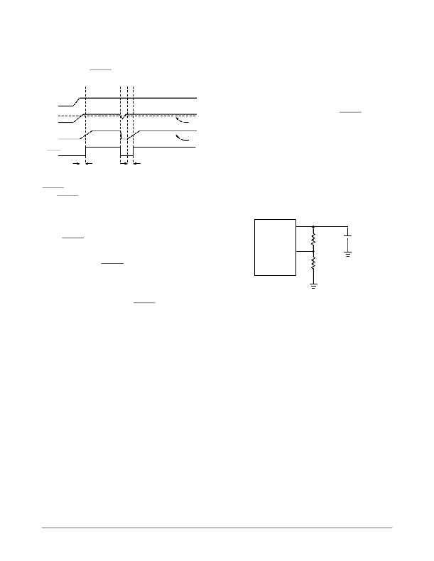
�Voltage� Adjust�
�Figure� 14� shows� the� device� setup� for� a� user� configurable�
�output� voltage.� The� feedback� to� the� V� ADJ� pin� is� taken� from�
�a� voltage� divider� referenced� to� the� output� voltage.� The� loop�
�is� balanced� around� the� Unity� Gain� threshold� (1.30� V�
�typical).�
�≈� 5.0� V�
�NCV8506� 15� k� C� OUT�
�controlled� by� a� low� voltage� detection� circuit.� The� circuit� is�
�functionally� independent� of� the� rest� of� the� IC� thereby�
�guaranteeing� that� the� RESET� signal� is� valid� for� V� OUT� as� low�
�as� 1.0� V.�
�DELAY� Function�
�V� ADJ�
�1.28� V�
�5.1� k�
�The� reset� delay� circuit� provides� a� programmable� (by�
�external� capacitor)� delay� on� the� RESET� output� lead.�
�APPLICATION� NOTES�
�Figure� 14.� Adjustable� Output�
�Voltage�
�SETTING� THE� DELAY� TIME�
�The� delay� time� is� controlled� by� the� Reset� Delay� Low�
�Voltage,� Delay� Switching� Threshold,� and� the� Delay� Charge�
�Current.� The� delay� follows� the� equation:�
�STABILITY� CONSIDERATIONS�
�The� output� or� compensation� capacitor� helps� determine�
�three� main� characteristics� of� a� linear� regulator:� start� ?� up�
�delay,� load� transient� response� and� loop� stability.�
�tDELAY� +�
�CDELAY(Vdt� *� Reset Delay Low Voltage)�
�Delay� Charge� Current�
�The� capacitor� value� and� type� should� be� based� on� cost,�
�availability,� size� and� temperature� constraints.� A� tantalum� or�
�aluminum� electrolytic� capacitor� is� best,� since� a� film� or�
�Example:�
�Using� C� DELAY� =� 33� nF.�
�Assume� reset� Delay� Low� Voltage� =� 0.�
�Use� the� typical� value� for� V� dt� =� 1.8� V� (2.5� V,� 3.3� V,� and�
�5.0� V� options).�
�Use� the� typical� value� for� Delay� Charge� Current� =� 4.2� m� A.�
�ceramic� capacitor� with� almost� zero� ESR� can� cause�
�instability.� The� aluminum� electrolytic� capacitor� is� the� least�
�expensive� solution,� but,� if� the� circuit� operates� at� low�
�temperatures� (� ?� 25� °� C� to� ?� 40� °� C),� both� the� value� and� ESR� of�
�the� capacitor� will� vary� considerably.� The� capacitor�
�manufacturers� data� sheet� usually� provides� this� information.�
�tDELAY� +�
�33 nF(1.8� *� 0)�
�4.2� m� A�
�+� 14� ms�
�http://onsemi.com�
�9�
�相关PDF资料 |
PDF描述 |
|---|---|
| XC18V512VQ44C | IC PROM SRL CONFIG 512K 44-VQFP |
| 1235L3X2 | BATTERY PK S-HD 9.0V C SIZE ZINC |
| R-78AA5.0-1.0SMD-R | CONV DC/DC 1A 5V OUT SMD |
| GBM25DSXH | CONN EDGECARD 50POS DIP .156 SLD |
| AT17LV512-10JC | IC SER CFG PROM 512K 3.3V 20PLCC |
相关代理商/技术参数 |
参数描述 |
|---|---|
| NCV8506D2TADJR4 | 功能描述:低压差稳压器 - LDO 400mA ADJ w/ENABLE RoHS:否 制造商:Texas Instruments 最大输入电压:36 V 输出电压:1.4 V to 20.5 V 回动电压(最大值):307 mV 输出电流:1 A 负载调节:0.3 % 输出端数量: 输出类型:Fixed 最大工作温度:+ 125 C 安装风格:SMD/SMT 封装 / 箱体:VQFN-20 |
| NCV8506D2TADJR4G | 功能描述:低压差稳压器 - LDO ANA MICROPOWER 400 RoHS:否 制造商:Texas Instruments 最大输入电压:36 V 输出电压:1.4 V to 20.5 V 回动电压(最大值):307 mV 输出电流:1 A 负载调节:0.3 % 输出端数量: 输出类型:Fixed 最大工作温度:+ 125 C 安装风格:SMD/SMT 封装 / 箱体:VQFN-20 |
| NCV8508 | 制造商:ONSEMI 制造商全称:ON Semiconductor 功能描述:5.0 V, 250 mA LDO with Watchdog and RESET |
| NCV85081BDS50G | 功能描述:低压差稳压器 - LDO 250 MA, 5 V, LDO RoHS:否 制造商:Texas Instruments 最大输入电压:36 V 输出电压:1.4 V to 20.5 V 回动电压(最大值):307 mV 输出电流:1 A 负载调节:0.3 % 输出端数量: 输出类型:Fixed 最大工作温度:+ 125 C 安装风格:SMD/SMT 封装 / 箱体:VQFN-20 |
| NCV85081BDS50R4G | 功能描述:低压差稳压器 - LDO 250 MA 5 V LDO RoHS:否 制造商:Texas Instruments 最大输入电压:36 V 输出电压:1.4 V to 20.5 V 回动电压(最大值):307 mV 输出电流:1 A 负载调节:0.3 % 输出端数量: 输出类型:Fixed 最大工作温度:+ 125 C 安装风格:SMD/SMT 封装 / 箱体:VQFN-20 |
发布紧急采购,3分钟左右您将得到回复。