- 您现在的位置:买卖IC网 > PDF目录19896 > NCV8509PDW18G (ON Semiconductor)IC REG LDO 3.3V/1.8V 16-SOIC PDF资料下载
参数资料
| 型号: | NCV8509PDW18G |
| 厂商: | ON Semiconductor |
| 文件页数: | 16/18页 |
| 文件大小: | 0K |
| 描述: | IC REG LDO 3.3V/1.8V 16-SOIC |
| 标准包装: | 47 |
| 稳压器拓扑结构: | 正,固定式 |
| 输出电压: | 3.3V,1.8V |
| 输入电压: | 最高 50V |
| 电压 - 压降(标准): | 0.4V @ 100mA |
| 稳压器数量: | 2 |
| 电流 - 限制(最小): | 115mA,105mA |
| 工作温度: | -40°C ~ 125°C |
| 安装类型: | 表面贴装 |
| 封装/外壳: | 16-SOIC(0.295",7.50mm 宽)裸露焊盘 |
| 供应商设备封装: | 16-SOIC W |
| 包装: | 管件 |
�� �
�
�NCV8509� Series�
�≈� 10� μ� s�
�V� OUT1�
�V� OUT2�
�≈� 10� μ� s�
�Fast� SLEW� Rate� >>� Soft� Start�
�Fast� SLEW� Rate� >>� Soft� Start�
�Disable� Time�
�Short� On�
�V� OUT1�
�Decay� Time� Dependent�
�on� External� Load�
�Disable� Time�
�Short� On�
�V� OUT2�
�Decay� Time� Dependent�
�on� External� Load�
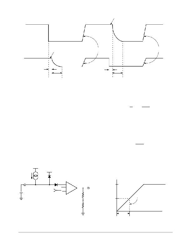
�Figure� 52.� Fault� Response.� Note� the� High� SLEW� Rate� Coming� Out� of� Fault� Conditions.�
�Soft� Start� Only� Applies� to� a� Power� Up� Sequence.�
�I� +� C� dv� ,� t� +�
�t� +�
�+� 9.9� ms�
�Av� +� OUT�
�Av� +�
�+� 3.9� V� V�
�Slew� Rate� Control�
�Figure� 53� shows� the� circuitry� associated� with� Slew� Rate�
�Control.� The� diagram� highlights� the� control� of� one� output� for�
�simplicity.� V� OUT1� and� V� OUT2� are� both� controlled� on� the� IC.�
�The� slew� rate� capacitor� (C� SLEW� )� is� charged� with� an�
�on� ?� chip� current� source� runing� at� 6.0� m� A� (typ.).� Charging� a�
�capacitor� with� a� current� source� creates� a� linear� voltage� ramp�
�as� shown� in� Figure� 54.�
�The� lowest� voltage� to� the� positive� terminals� of� the�
�comparator� (Error� Amp)� dominates� the� output� voltage�
�(V� OUT� ).� Consequently,� when� C� SLEW� is� fully� discharged� on�
�power� up,� it� is� the� dominant� factor� on� the� positive� terminal�
�and� disables� the� output.� The� output� (V� OUT� )� follows� the�
�linear� ramp� on� the� SLEW� pin� (after� being� gained� up� with� R1�
�and� R2)� until� V� BG� becomes� the� dominant� voltage.� This�
�occurs� when� SLEW� =� V� BG� +� V� D1� or� approximately� 1.8� V.�
�Internal�
�Slew� time� can� be� calculated� using� the� standard� capacitor�
�equation.�
�C(� D� V)�
�dt� I�
�Using� a� 33� nF� capacitor,� the� slew� time� is:�
�(33 nF)(1.8 V)�
�6� m� A�
�The� corresponding� slew� rate� for� this� is� 1.8� V/9.9� ms� =�
�182� V/s� ON� THE� SLEW� PIN.�
�To� calculate� the� slew� rate� on� outputs,� you� must� multiply�
�by� the� gain� set� up� by� R1� and� R2.�
�V�
�1.28� V�
�For� a� 5� V� output,� the� gain� would� be:�
�5V�
�1.28� V�
�Voltage�
�Rail� ≈� 3.8� V�
�V� IN1�
�assuming� V� BG� =� 1.28� V.�
�The� resultant� slew� rate� on� the� output� is� the� slew� rate� on� the�
�SLEW� pin� multiplied� by� the� gain,� or:�
�6.0� μ� A�
�D2�
�(182� V� s)�
�(3.9� V� V)� +� 710� V� s�
�SLEW�
�C� SLEW�
�V� BG�
�D1�
�+�
�+�
�?�
�Error� Amp�
�V� OUT�
�R1�
�3.8�
�1.8�
�Outputs� in� Regulation�
�R2�
�t� SLEW�
�Figure� 53.� Slew� Control� Circuitry�
�http://onsemi.com�
�16�
�Time� (ms)�
�Figure� 54.�
�相关PDF资料 |
PDF描述 |
|---|---|
| T97R106M075ESS | CAP TANT 10UF 75V 20% 3024 |
| CDRH125/LDNP-220MC | POWER INDUCTOR 22UH 3.28A SMD |
| AT17LV010A-10QC | IC CONFIG SEEPROM 1M 3.3V 32TQFP |
| LTC4302CMS-2#PBF | IC BUS BUFFER 2-WIRE 10-MSOP |
| EMA50DRSD-S288 | CONN EDGECARD 100POS .125 EXTEND |
相关代理商/技术参数 |
参数描述 |
|---|---|
| NCV8509PDW18R2 | 功能描述:线性稳压器 - 标准 1.8V 100mA Sequenced RoHS:否 制造商:STMicroelectronics 输出类型: 极性: 输出电压:1.8 V 输出电流:150 mA 负载调节: 最大输入电压:5.5 V 线路调整率: 最大工作温度:+ 125 C 安装风格:SMD/SMT 封装 / 箱体:SOT-323-5L |
| NCV8509PDW18R2G | 功能描述:线性稳压器 - 标准 1.8V 100mA Sequenced Dual RoHS:否 制造商:STMicroelectronics 输出类型: 极性: 输出电压:1.8 V 输出电流:150 mA 负载调节: 最大输入电压:5.5 V 线路调整率: 最大工作温度:+ 125 C 安装风格:SMD/SMT 封装 / 箱体:SOT-323-5L |
| NCV8509PDW25 | 功能描述:线性稳压器 - 标准 2.5V 100mA Sequenced RoHS:否 制造商:STMicroelectronics 输出类型: 极性: 输出电压:1.8 V 输出电流:150 mA 负载调节: 最大输入电压:5.5 V 线路调整率: 最大工作温度:+ 125 C 安装风格:SMD/SMT 封装 / 箱体:SOT-323-5L |
| NCV8509PDW25G | 功能描述:线性稳压器 - 标准 2.5V 100mA Sequenced Dual RoHS:否 制造商:STMicroelectronics 输出类型: 极性: 输出电压:1.8 V 输出电流:150 mA 负载调节: 最大输入电压:5.5 V 线路调整率: 最大工作温度:+ 125 C 安装风格:SMD/SMT 封装 / 箱体:SOT-323-5L |
| NCV8509PDW25R2 | 功能描述:线性稳压器 - 标准 2.5V 100mA Sequenced RoHS:否 制造商:STMicroelectronics 输出类型: 极性: 输出电压:1.8 V 输出电流:150 mA 负载调节: 最大输入电压:5.5 V 线路调整率: 最大工作温度:+ 125 C 安装风格:SMD/SMT 封装 / 箱体:SOT-323-5L |
发布紧急采购,3分钟左右您将得到回复。