- 您现在的位置:买卖IC网 > PDF目录20083 > NCV8535MN285R2G (ON Semiconductor)IC REG LDO 2.85V .7A 10-DFN PDF资料下载
参数资料
| 型号: | NCV8535MN285R2G |
| 厂商: | ON Semiconductor |
| 文件页数: | 4/22页 |
| 文件大小: | 0K |
| 描述: | IC REG LDO 2.85V .7A 10-DFN |
| 标准包装: | 3,000 |
| 稳压器拓扑结构: | 正,固定式 |
| 输出电压: | 2.85V |
| 输入电压: | 3.25 V ~ 12 V |
| 稳压器数量: | 1 |
| 电流 - 输出: | 700mA |
| 工作温度: | -40°C ~ 85°C |
| 安装类型: | 表面贴装 |
| 封装/外壳: | 10-VFDFN 裸露焊盘 |
| 供应商设备封装: | 10-DFN(3x3) |
| 包装: | 带卷 (TR) |
��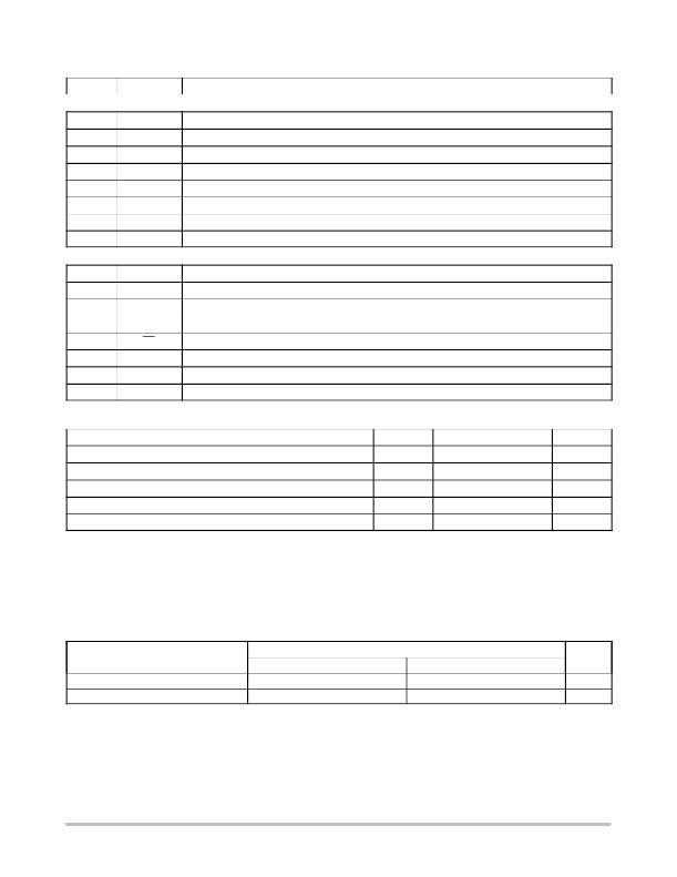 �
�
�NCV8535�
�PIN� FUNCTION� DESCRIPTION�
�Pin� No.�
�Pin� Name�
�Description�
�FIXED� VERSION�
�1,� 2�
�3�
�4�
�7�
�8�
�9,� 10�
�5,� 6�
�EPAD�
�V� out�
�SENSE�
�GND�
�NR�
�SD�
�V� in�
�NC�
�EPAD�
�Regulated� output� voltage.� Bypass� to� ground� with� C� out� w� 1.0� m� F.�
�For� output� voltage� sensing,� connect� to� Pins� 1� and� 2.�
�Power� Supply� Ground�
�Noise� Reduction� Pin.� This� is� an� optional� pin� used� to� further� reduce� noise.�
�Shutdown� pin.� When� not� in� use,� this� pin� should� be� connected� to� the� input� pin.�
�Power� Supply� Input� Voltage�
�Not� Connected�
�Exposed� thermal� pad� should� be� connected� to� ground.�
�ADJUSTABLE� VERSION�
�1,� 2�
�3�
�4�
�7�
�8�
�9,� 10�
�5,� 6�
�EPAD�
�V� out�
�Adj�
�GND�
�NR�
�SD�
�V� in�
�NC�
�EPAD�
�Regulated� output� voltage.� Bypass� to� ground� with� C� out� w� 1.0� m� F.�
�Adjustable� pin;� reference� voltage� =� 1.25� V.�
�Power� Supply� Ground�
�Noise� Reduction� Pin.� This� is� an� optional� pin� used� to� further� reduce� noise.�
�Shutdown� pin.� When� not� in� use,� this� pin� should� be� connected� to� the� input� pin.�
�Power� Supply� Input� Voltage�
�Not� Connected�
�Exposed� thermal� pad� should� be� connected� to� ground.�
�MAXIMUM� RATINGS�
�Input� Voltage�
�Output� Voltage�
�Shutdown� Pin� Voltage�
�Junction� Temperature� Range�
�Storage� Temperature� Range�
�Rating�
�Symbol�
�V� in�
�V� out�
�V� sh�
�T� J�
�T� stg�
�Value�
�?� 0.3� to� +16�
�?� 0.3� to� V� in� +0.3� or� 10� V*�
�?� 0.3� to� +16�
�?� 40� to� +150�
�?� 55� to� +150�
�Unit�
�V�
�V�
�V�
�?� C�
�?� C�
�Stresses� exceeding� Maximum� Ratings� may� damage� the� device.� Maximum� Ratings� are� stress� ratings� only.� Functional� operation� above� the�
�Recommended� Operating� Conditions� is� not� implied.� Extended� exposure� to� stresses� above� the� Recommended� Operating� Conditions� may� affect�
�device� reliability.�
�NOTE:� This� device� series� contains� ESD� protection� and� exceeds� the� following� tests:�
�Human� Body� Model� (HBM)� tested� per� AEC� ?� Q100� ?� 002� (EIA/JESD22� ?� A114)�
�Machine� Model� (MM)� tested� per� AEC� ?� Q100� ?� 003� (EIA/JESD22� ?� A115)�
�Charged� Device� Model� (CDM)� tested� per� EIA/JESD22� ?� C101�
�*Which� ever� is� less.� Reverse� bias� protection� feature� valid� only� if� V� out� ?� V� in� ?� 7� V.�
�THERMAL� CHARACTERISTICS�
�Test� Conditions� (Typical� Value)�
�Characteristic�
�Junction� ?� to� ?� Air,� q� JA�
�Junction� ?� to� ?� Pin,� y� JL2�
�Min� Pad� Board� (Note� 1)�
�215�
�55�
�1� ,� Pad� Board� (Note� 1)�
�66�
�17�
�Unit�
�?� C/W�
�?� C/W�
�1.� As� mounted� on� a� 35� x� 35� x� 1.5� mm� FR4� Substrate,� with� a� single� layer� of� a� specified� copper� area� of� 2� oz� (0.07� mm� thick)� copper� traces� and�
�heat� spreading� area.� JEDEC� 51� specifications� for� a� low� and� high� conductivity� test� board� recommend� a� 2� oz� copper� thickness.� Test� conditions�
�are� under� natural� convection� or� zero� air� flow.�
�http://onsemi.com�
�4�
�相关PDF资料 |
PDF描述 |
|---|---|
| TPSC107K006R0075 | CAP TANT 100UF 6.3V 10% 2312 |
| CENB1020A1403B01 | POWER SUPPLY EXT 16.8W 14V @1.2A |
| T86D226M016EAAS | CAP TANT 22UF 16V 20% 2917 |
| ACM25DTMN-S189 | CONN EDGECARD 50POS R/A .156 SLD |
| T86D226K016EAAS | CAP TANT 22UF 16V 10% 2917 |
相关代理商/技术参数 |
参数描述 |
|---|---|
| NCV8535MN300R2G | 功能描述:低压差稳压器 - LDO 500mA LDO AUTO VERSN RoHS:否 制造商:Texas Instruments 最大输入电压:36 V 输出电压:1.4 V to 20.5 V 回动电压(最大值):307 mV 输出电流:1 A 负载调节:0.3 % 输出端数量: 输出类型:Fixed 最大工作温度:+ 125 C 安装风格:SMD/SMT 封装 / 箱体:VQFN-20 |
| NCV8535MN330R2G | 功能描述:低压差稳压器 - LDO 500mA LDO AUTO VERSN RoHS:否 制造商:Texas Instruments 最大输入电压:36 V 输出电压:1.4 V to 20.5 V 回动电压(最大值):307 mV 输出电流:1 A 负载调节:0.3 % 输出端数量: 输出类型:Fixed 最大工作温度:+ 125 C 安装风格:SMD/SMT 封装 / 箱体:VQFN-20 |
| NCV8535MN350R2G | 功能描述:IC REG LDO 3.5V .7A 10-DFN RoHS:是 类别:集成电路 (IC) >> PMIC - 稳压器 - 线性 系列:- 标准包装:1 系列:- 稳压器拓扑结构:正,可调式 输出电压:1.25 V ~ 10 V 输入电压:2.9 V ~ 12 V 电压 - 压降(标准):- 稳压器数量:1 电流 - 输出:700mA 电流 - 限制(最小):- 工作温度:-40°C ~ 85°C 安装类型:表面贴装 封装/外壳:10-VFDFN 裸露焊盘 供应商设备封装:10-DFN(3x3) 包装:Digi-Reel® 其它名称:NCV8535MNADJR2GOSDKR |
| NCV8535MN500R2G | 功能描述:低压差稳压器 - LDO 500mA LDO AUTO VERSN RoHS:否 制造商:Texas Instruments 最大输入电压:36 V 输出电压:1.4 V to 20.5 V 回动电压(最大值):307 mV 输出电流:1 A 负载调节:0.3 % 输出端数量: 输出类型:Fixed 最大工作温度:+ 125 C 安装风格:SMD/SMT 封装 / 箱体:VQFN-20 |
| NCV8535MN500R2G/H | 制造商:ON Semiconductor 功能描述: |
发布紧急采购,3分钟左右您将得到回复。