参数资料
| 型号: | NCV8570BSN18T1G |
| 厂商: | ON Semiconductor |
| 文件页数: | 17/20页 |
| 文件大小: | 0K |
| 描述: | IC REG LDO 1.8V .2A 5TSOP |
| 标准包装: | 1 |
| 稳压器拓扑结构: | 正,固定式 |
| 输出电压: | 1.8V |
| 输入电压: | 2.5 V ~ 5.5 V |
| 稳压器数量: | 1 |
| 电流 - 输出: | 200mA |
| 电流 - 限制(最小): | 200mA |
| 工作温度: | -40°C ~ 125°C |
| 安装类型: | 表面贴装 |
| 封装/外壳: | 6-TSOP(0.059",1.50mm 宽)5 引线 |
| 供应商设备封装: | 5-TSOP |
| 包装: | 标准包装 |
| 其它名称: | NCV8570BSN18T1GOSDKR |
�� �
�
�NCV8570B�
�P� D(MAX)� +�
�Such� condition� could� exist� in� the� case� of� pulling� the� V� IN�
�voltage� to� ground.� Then� the� output� capacitor� voltage� will� be�
�partially� discharged� through� the� PMOS� body� diode.� It� have�
�been� verified� that� the� device� will� not� be� damaged� if� the�
�output� capacitance� is� less� than� 22� m� F.� If� however� larger�
�output� capacitors� are� used� or� extended� reverse� current�
�condition� is� anticipated� the� device� may� require� additional�
�external� protection� against� the� excessive� reverse� current.�
�Output� Noise�
�If� we� neglect� the� noise� coming� from� the� (IN)� input� pin� of�
�the� LDO,� the� main� contributor� of� noise� present� on� the� output�
�pin� (OUT)� is� the� internal� bandgap� reference.� This� is� because�
�any� noise� which� is� generated� at� this� node� will� be�
�subsequently� amplified� through� the� error� amplifier� and� the�
�PMOS� pass� device.� Access� to� the� bandgap� reference� node� is�
�supplied� through� the� BYP� pin.� For� the� 1.8� V� output� voltage�
�100� nF� from� the� BYP� pin� to� ground.� For� more� information�
�please� refer� to� Figures� 22� through� 24.�
�Minimum� Load� Current�
�NCV8570B� does� not� require� any� minimum� load� current�
�for� stability.� The� minimum� load� current� is� assured� by� the�
�internal� circuitry.�
�Power� Dissipation�
�For� given� ambient� temperature� T� A� and� thermal� resistance�
�R� q� JA� the� maximum� device� power� dissipation� can� be�
�calculated� by:�
�T� J(MAX)� *� T� A�
�(eq.� 2)�
�q� JA�
�The� actual� power� dissipation� can� be� calculated� by� the�
�formula:�
�option� Noise� can� be� reduced� from� a� typical� value� of�
�15� m� Vrms� by� using� 10� nF� to� less� than� 10� m� Vrms� by� using� a�
�P� D� +� V� IN� *� V� OUT� I� OUT� )� V� IN� I� GND�
�(eq.� 3)�
�310�
�290�
�270�
�250�
�230�
�210�
�190�
�P� D(MAX)� ,� T� A� =� 25� ?� C,�
�2� oz� Cu� Thickness�
�P� D(MAX)� ,� T� A� =� 25� ?� C,�
�1� oz� Cu� Thickness�
�q� JA� ,� 1� oz� Cu� Thickness�
�0.60�
�0.55�
�0.50�
�0.45�
�0.40�
�0.35�
�0.30�
�240�
�220�
�200�
�180�
�160�
�140�
�120�
�P� D(MAX)� ,� T� A� =� 25� ?� C,�
�2� oz� Cu� Thickness�
�P� D(MAX)� ,� T� A� =� 25� ?� C,�
�1� oz� Cu� Thickness�
�1.20�
�1.10�
�1.00�
�0.90�
�0.80�
�0.70�
�0.60�
�q� JA� ,� 2� oz� Cu� Thickness�
�q� JA� ,� 2� oz� Cu� Thickness�
�170� 0.25�
�150� 0.20�
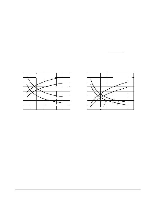
�0� 100� 200� 300� 400� 500� 600� 700�
�PCB� COPPER� AREA� (mm� 2� )�
�Figure� 57.� Thermal� Resistance� and� Maximum�
�Power� Dissipation� vs.� Copper� Area� (TSOP� ?� 5)�
�Load� Regulation�
�The� NCV8570B� features� very� good� load� regulation� of�
�5� mV� Max.� in� 0� mA� to� 200� mA� range.� In� order� to� achieve�
�this� very� good� load� regulation� a� special� attention� to� PCB�
�design� is� necessary.� The� trace� resistance� from� the� OUT� pin�
�to� the� point� of� load� can� easily� approach� 100� m� W� which� will�
�cause� 20� mV� voltage� drop� at� full� load� current,� deteriorating�
�the� excellent� load� regulation.�
�Line� Regulation�
�The� NCV8570B� features� very� good� line� regulation� of�
�0.6mV/V� (typ).� Furthermore� the� detailed� Output� Voltage� vs.�
�Input� Voltage� characteristics� (Figures� 47� through� 49)� show�
�that� up� to� V� IN� =� 5� V� the� Output� Voltage� deviation� is� typically�
�less� than� 250� m� V� for� 1.8� V� output� voltage� option� and� less�
�than� 150� m� V� for� higher� output� voltage� options.� Above� the�
�V� IN� =� 5� V� the� output� voltage� falls� rapidly� which� leads� to� the�
�typical� 0.6� mV/V.�
�100� 0.50�
�q� JA� ,� 1� oz� Cu� Thickness�
�80� 0.40�
�0� 100� 200� 300� 400� 500� 600� 700�
�PCB� COPPER� AREA� (mm� 2� )�
�Figure� 58.� Thermal� Resistance� and� Maximum�
�Power� Dissipation� vs.� Copper� Area� (DFN6)�
�In� the� frequency� range� from� 10� Hz� up� to� about� 10� kHz� the�
�larger� noise� bypass� capacitor� C� noise� will� help� to� improve� the�
�PSRR.� At� the� frequencies� above� 10� kHz� the� addition� of�
�higher� C� OUT� output� capacitor� will� result� in� improved� PSRR.�
�PCB� Layout� Recommendations�
�Connect� the� input� (C� IN� ),� output� (C� OUT� )� and� noise� bypass�
�capacitors� (C� noise� )� as� close� as� possible� to� the� device� pins.�
�The� C� noise� capacitor� is� connected� to� high� impedance� BYP�
�pin� and� thus� the� length� of� the� trace� between� the� capacitor� and�
�the� pin� should� be� as� small� as� possible� to� avoid� noise� pickup.�
�In� order� to� minimize� the� solution� size� use� 0402� or� 0603�
�capacitors.� To� obtain� small� transient� variations� and� good�
�regulation� characteristics� place� C� IN� and� C� OUT� capacitors�
�close� to� the� device� pins� and� make� the� PCB� traces� wide.�
�Larger� copper� area� connected� to� the� pins� will� also� improve�
�the� device� thermal� resistance.�
�Power� Supply� Rejection� Ratio�
�The� NCV8570B� features� excellent� Power� Supply�
�Rejection� ratio.� The� PSRR� can� be� tuned� by� selecting� proper�
�C� noise� and� C� OUT� capacitors.�
�http://onsemi.com�
�17�
�相关PDF资料 |
PDF描述 |
|---|---|
| IDT72V51443L7-5BBI | IC FLOW CTRL MULTI QUEUE 256-BGA |
| LFXP10E-4FN256I | IC FPGA 9.7KLUTS 256FPBGA |
| LFXP10E-5FN256C | IC FPGA 9.7KLUTS 188I/O 256-BGA |
| LFXP10C-5FN256C | IC FPGA 9.7KLUTS 188I/O 256-BGA |
| GCB75DHBN | CONN EDGECARD 150PS R/A .050 SLD |
相关代理商/技术参数 |
参数描述 |
|---|---|
| NCV8570BSN25T1G | 功能描述:低压差稳压器 - LDO 200MA ULN RF LDO REG2.5V RoHS:否 制造商:Texas Instruments 最大输入电压:36 V 输出电压:1.4 V to 20.5 V 回动电压(最大值):307 mV 输出电流:1 A 负载调节:0.3 % 输出端数量: 输出类型:Fixed 最大工作温度:+ 125 C 安装风格:SMD/SMT 封装 / 箱体:VQFN-20 |
| NCV8570BSN28T1G | 功能描述:低压差稳压器 - LDO 200MA ULN RF LDO REG2.8V RoHS:否 制造商:Texas Instruments 最大输入电压:36 V 输出电压:1.4 V to 20.5 V 回动电压(最大值):307 mV 输出电流:1 A 负载调节:0.3 % 输出端数量: 输出类型:Fixed 最大工作温度:+ 125 C 安装风格:SMD/SMT 封装 / 箱体:VQFN-20 |
| NCV8570BSN30T1G | 功能描述:低压差稳压器 - LDO 200MA ULN RF LDO REG 3V RoHS:否 制造商:Texas Instruments 最大输入电压:36 V 输出电压:1.4 V to 20.5 V 回动电压(最大值):307 mV 输出电流:1 A 负载调节:0.3 % 输出端数量: 输出类型:Fixed 最大工作温度:+ 125 C 安装风格:SMD/SMT 封装 / 箱体:VQFN-20 |
| NCV8570BSN33T1G | 功能描述:低压差稳压器 - LDO 200MA ULN RF LDO REG3.3V RoHS:否 制造商:Texas Instruments 最大输入电压:36 V 输出电压:1.4 V to 20.5 V 回动电压(最大值):307 mV 输出电流:1 A 负载调节:0.3 % 输出端数量: 输出类型:Fixed 最大工作温度:+ 125 C 安装风格:SMD/SMT 封装 / 箱体:VQFN-20 |
| NCV8570MN180R2G | 功能描述:低压差稳压器 - LDO RF LDO / 150 mA RoHS:否 制造商:Texas Instruments 最大输入电压:36 V 输出电压:1.4 V to 20.5 V 回动电压(最大值):307 mV 输出电流:1 A 负载调节:0.3 % 输出端数量: 输出类型:Fixed 最大工作温度:+ 125 C 安装风格:SMD/SMT 封装 / 箱体:VQFN-20 |
发布紧急采购,3分钟左右您将得到回复。