- 您现在的位置:买卖IC网 > PDF目录20707 > NCV8668ABD133R2G (ON Semiconductor)IC REG LDO 3.3V .15A 8-SOIC PDF资料下载
参数资料
| 型号: | NCV8668ABD133R2G |
| 厂商: | ON Semiconductor |
| 文件页数: | 14/18页 |
| 文件大小: | 0K |
| 描述: | IC REG LDO 3.3V .15A 8-SOIC |
| 标准包装: | 2,500 |
| 稳压器拓扑结构: | 正,固定式 |
| 输出电压: | 3.3V |
| 输入电压: | 4.5 V ~ 40 V |
| 稳压器数量: | 1 |
| 电流 - 输出: | 150mA |
| 电流 - 限制(最小): | 205mA |
| 工作温度: | -40°C ~ 150°C |
| 安装类型: | 表面贴装 |
| 封装/外壳: | 8-SOIC(0.154",3.90mm 宽) |
| 供应商设备封装: | 8-SOICN |
| 包装: | 带卷 (TR) |
�� �
�
�NCV8668�
�T� J(MAX)� *� T� A�
�P� D(MAX)� +�
�a� pull� ?� up� resistor� (30� k� W� )� internally� connected� to� the� output�
�(V� OUT� ).� No� external� pull� ?� up� is� necessary.�
�For� voltage� option� 3.3� V� RO� is� open� drain� output� and�
�external� pull� ?� up� resistor� is� required.�
�Reset� signal� is� also� generated� in� case� when� input� voltage�
�decreases� below� its� minimum� operating� limit� (4.5� V).� The�
�Input� Voltage� Reset� Threshold� is� typically� 3.8� V.� This�
�applies� only� to� voltage� options� with� nominal� value� below�
�minimum� operating� input� voltage� (3.3� V).�
�Window� Watchdog� Operation�
�The� watchdog� slow,� fast� or� off� state� is� set� by� pins� WM1�
�and� WM2� (see� table� in� Figure� 25).� The� timing� values� used�
�in� this� description� refer� to� typ.� Values� when� WM1� and� WM2�
�are� connected� to� GND� (fast� watchdog� and� reset� timing).� The�
�affect� the� rate� of� junction� temperature� rise� for� the� part.� When�
�the� NCV8668� has� good� thermal� conductivity� through� the�
�PCB,� the� junction� temperature� will� be� relatively� low� with�
�high� power� applications.� The� maximum� dissipation� the�
�NCV8668� can� handle� is� given� by:�
�(eq.� 1)�
�R� q� JA�
�Since� T� J� is� not� recommended� to� exceed� 150� °� C,� then� the�
�NCV8668� soldered� on� 645� mm� 2� ,� 1� oz� copper� area,� FR4� can�
�dissipate� up� to� 1.3� W� for� SOIC� ?� 14� package� when� the�
�ambient� temperature� (T� A� )� is� 25� °� C.� See� Figure� 28� for� R� q� JA�
�versus� PCB� area.� The� power� dissipated� by� the� NCV8668� can�
�be� calculated� from� the� following� equations:�
�state� diagram� of� the� window� watchdog� (WWD)� and� the�
�watchdog� and� reset� mode� selection� table� is� shown� in�
�Figure� 25.� The� WWD� timing� is� shown� in� Figure� 26.� After�
�or�
�P� D� +� V� in� I� q� @I� out� )� I� out� V� in� *� V� out�
�(eq.� 2)�
�power� ?� on,� the� reset� output� signal� at� the� RO� pin�
�(microprocessor� reset)� is� kept� LOW� for� the� reset� delay� time�
�t� RD� (16� ms).� RO� signal� transition� from� LOW� to� HIGH�
�triggers� the� ignore� window� (IW)� with� duration� of� t� IW�
�(32� ms).� During� this� window� the� signal� at� the� WDI� pin� is�
�140�
�V� in(MAX)� +�
�P� D(MAX)� )� V� out�
�I� out� )� I� q�
�I� out�
�(eq.� 3)�
�ignored.� When� IW� ends� a� long� open� window� with� maximum�
�duration� of� (128� ms,� t� max� =� 4xt� OW� )� is� started.� When� a� valid�
�trigger� signal� is� detected� during� long� open� window,� a� closed�
�window� (CW)� with� duration� of� t� CW� (32� ms)� is� initialized�
�immediately.� WDI� signal� transition� from� HIGH� to� LOW� is�
�taken� as� a� trigger.� As� valid� trigger� two� HIGH� samples�
�followed� by� two� LOW� samples� (with� sampling� time� t� sam� =�
�0.5� ms)� have� to� be� present� before� end� of� the� long� window.�
�Valid� WDI� trigger� signal� is� shown� in� Figure� 27.� When� CW�
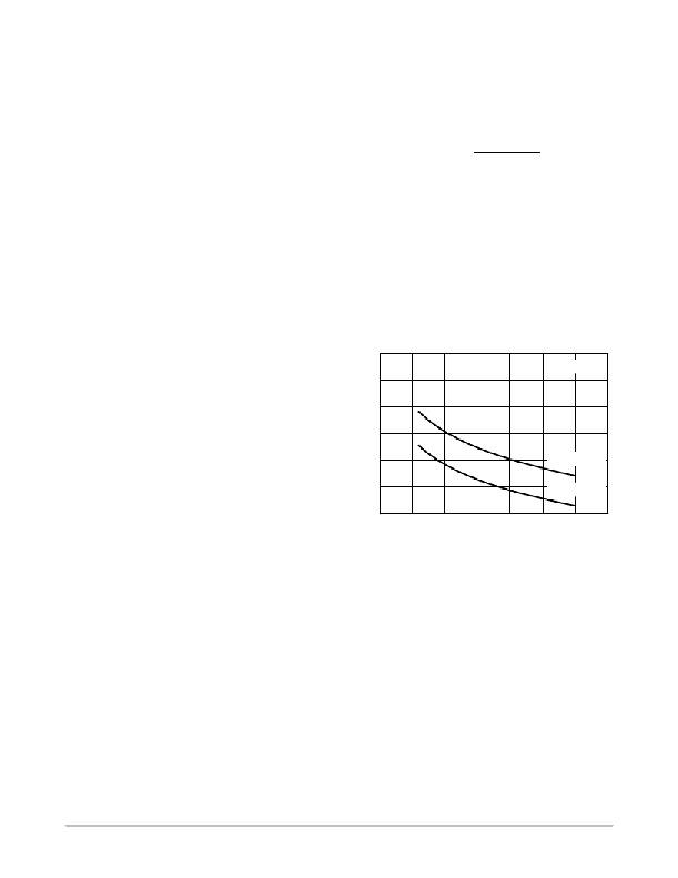
�130�
�120�
�110�
�100�
�SOIC� ?� 14�
�PCB� 1� oz� Cu�
�PCB� 2� oz� Cu�
�ends� a� standard� open� window� (OW)� with� maximum� duration�
�of� t� OW� (32� ms)� is� initiated� immediately.� The� OW� ends�
�immediately� when� valid� trigger� appears� at� WDI� input.� For�
�normal� operation� the� microprocessor� timing� of� WDI� pulses�
�must� be� stable� and� correspond� to� t� WD� .� A� reset� signal� is�
�generated� (RO� goes� LOW)� if� there� is� no� valid� trigger�
�(missing� pulse� at� WDI� pin)� during� OW� or� if� a� pre� ?� trigger�
�occurs� during� the� CW� (unexpected� pulse� at� WDI� pin).�
�Thermal� Considerations�
�As� power� in� the� NCV8668� increases,� it� might� become�
�necessary� to� provide� some� thermal� relief.� The� maximum�
�power� dissipation� supported� by� the� device� is� dependent�
�upon� board� design� and� layout.� Mounting� pad� configuration�
�on� the� PCB,� the� board� material,� and� the� ambient� temperature�
�90�
�80�
�0� 100� 200� 300� 400� 500� 600� 700�
�COPPER� HEAT� SPREADER� AREA� (mm� 2� )�
�Figure� 28.� Thermal� Resistance� vs� PCB� Copper� Area�
�Hints�
�V� in� and� GND� printed� circuit� board� traces� should� be� as�
�wide� as� possible.� When� the� impedance� of� these� traces� is�
�high,� there� is� a� chance� to� pick� up� noise� or� cause� the� regulator�
�to� malfunction.� Place� external� components,� especially� the�
�output� capacitor,� as� close� as� possible� to� the� NCV8668,� and�
�make� traces� as� short� as� possible.�
�http://onsemi.com�
�14�
�相关PDF资料 |
PDF描述 |
|---|---|
| NCP508MT15TBG | IC REG LDO 1.5V 50MA WDFN6 |
| ACB66DHFD-S621 | EDGECARD 132POS SMD W/O POST |
| TPSE108M004R0040 | CAP TANT 1000UF 4V 20% 2917 |
| VE-J3X-EW-B1 | CONVERTER MOD DC/DC 5.2V 100W |
| ECM15DCBI | CONN EDGECARD 30POS R/A .156 SLD |
相关代理商/技术参数 |
参数描述 |
|---|---|
| NCV8668ABD150R2G | 功能描述:低压差稳压器 - LDO 5.0V/150MA LDO RoHS:否 制造商:Texas Instruments 最大输入电压:36 V 输出电压:1.4 V to 20.5 V 回动电压(最大值):307 mV 输出电流:1 A 负载调节:0.3 % 输出端数量: 输出类型:Fixed 最大工作温度:+ 125 C 安装风格:SMD/SMT 封装 / 箱体:VQFN-20 |
| NCV8668ABD250R | 制造商:ON Semiconductor 功能描述: |
| NCV8668ABD250R2G | 功能描述:直流/直流开关转换器 150 MA LDO REGULATOR RoHS:否 制造商:STMicroelectronics 最大输入电压:4.5 V 开关频率:1.5 MHz 输出电压:4.6 V 输出电流:250 mA 输出端数量:2 最大工作温度:+ 85 C 安装风格:SMD/SMT |
| NCV8668ABPD33R2G | 功能描述:低压差稳压器 - LDO 3.3V/150 MA LDO RoHS:否 制造商:Texas Instruments 最大输入电压:36 V 输出电压:1.4 V to 20.5 V 回动电压(最大值):307 mV 输出电流:1 A 负载调节:0.3 % 输出端数量: 输出类型:Fixed 最大工作温度:+ 125 C 安装风格:SMD/SMT 封装 / 箱体:VQFN-20 |
| NCV8668ABPD50R2G | 功能描述:低压差稳压器 - LDO 5.0V/150MA LDO RoHS:否 制造商:Texas Instruments 最大输入电压:36 V 输出电压:1.4 V to 20.5 V 回动电压(最大值):307 mV 输出电流:1 A 负载调节:0.3 % 输出端数量: 输出类型:Fixed 最大工作温度:+ 125 C 安装风格:SMD/SMT 封装 / 箱体:VQFN-20 |
发布紧急采购,3分钟左右您将得到回复。