- 您现在的位置:买卖IC网 > PDF目录13649 > NCV8842PWG (ON Semiconductor)IC REG BUCK 1.5A 16SOIC PDF资料下载
参数资料
| 型号: | NCV8842PWG |
| 厂商: | ON Semiconductor |
| 文件页数: | 9/16页 |
| 文件大小: | 0K |
| 描述: | IC REG BUCK 1.5A 16SOIC |
| 标准包装: | 47 |
| 类型: | 降压(降压) |
| 输出数: | 1 |
| 输入电压: | 4.5 V ~ 40 V |
| PWM 型: | 混合物 |
| 频率 - 开关: | 170kHz |
| 电流 - 输出: | 1.5A |
| 同步整流器: | 无 |
| 工作温度: | -40°C ~ 150°C |
| 安装类型: | 表面贴装 |
| 封装/外壳: | 16-SOIC(0.295",7.50mm 宽)裸露焊盘 |
| 包装: | 管件 |
| 供应商设备封装: | 16-SOIC W |
�� �
�
�NCV8842�
�Startup�
�During� power� up,� the� regulator� tends� to� quickly� charge� up�
�the� output� capacitors� to� reach� voltage� regulation.� This� gives�
�rise� to� an� excessive� in� ?� rush� current� which� can� be� detrimental�
�to� the� inductor,� IC� and� catch� diode.� In� V� 2� control� ,� the�
�compensation� capacitor� provides� Soft� ?� Start� with� no� need�
�for� extra� pin� or� circuitry.� During� the� power� up,� the� Output�
�Source� Current� of� the� error� amplifier� charges� the�
�compensation� capacitor� which� forces� V� C� pin� and� thus� output�
�voltage� ramp� up� gradually.� The� Soft� ?� Start� duration� can� be�
�calculated� by�
�minimum� duty� cycle� by� extending� the� switching� cycle.� This�
�protects� the� IC� from� overheating,� and� also� limits� the� power�
�that� can� be� transferred� to� the� output.� The� current� limit�
�foldback� effectively� reduces� the� current� stress� on� the�
�inductor� and� diode.� When� the� output� is� shorted,� the� DC�
�current� of� the� inductor� and� diode� can� approach� the� current�
�limit� threshold.� Therefore,� reducing� the� current� limit� by�
�40%� can� result� in� an� equal� percentage� drop� of� the� inductor�
�and� diode� current.� The� short� circuit� waveforms� are� captured�
�in� Figure� 12,� and� the� benefit� of� the� foldback� frequency� and�
�current� limit� is� self� ?� evident.�
�TSS� +� C�
�V CCOMP�
�ISOURCE�
�where:�
�V� C� =� V� C� pin� steady� ?� state� voltage,� which� is� approximately�
�equal� to� error� amplifier� ’s� reference� voltage.�
�C� COMP� =� Compensation� capacitor� connected� to� the� V� C� pin�
�I� SOURCE� =� Output� Source� Current� of� the� error� amplifier.�
�Using� a� 0.1� m� F� C� COMP� ,� the� calculation� shows� a� T� SS� over�
�5.0� ms� which� is� adequate� to� avoid� any� current� stresses.�
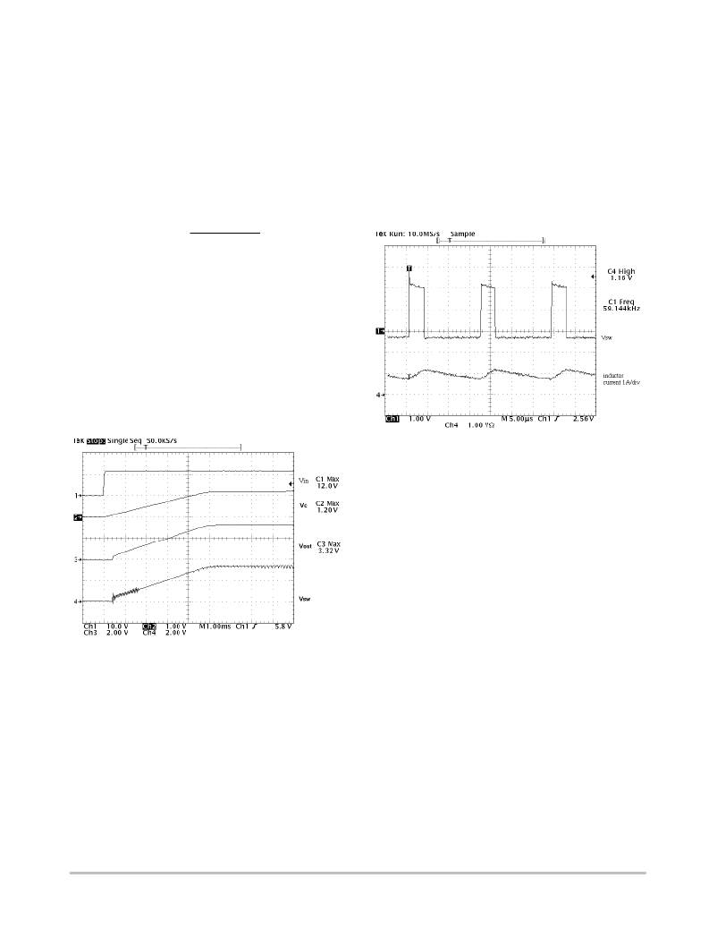
�Figure� 11� shows� the� gradual� rise� of� the� V� C� ,� V� O� and� envelope�
�of� the� V� SW� during� power� up.� There� is� no� voltage� over� ?� shoot�
�after� the� output� voltage� reaches� the� regulation.� If� the� supply�
�voltage� rises� slower� than� the� V� C� pin,� output� voltage� may�
�over� ?� shoot.�
�Figure� 12.� In� Short� Circuit,� the� Foldback� Current� and�
�Foldback� Frequency� Limit� the� Switching� Current� to�
�Protect� the� IC,� Inductor� and� Catch� Diode�
�Thermal� Considerations�
�A� calculation� of� the� power� dissipation� of� the� IC� is� always�
�necessary� prior� to� the� adoption� of� the� regulator.� The� current�
�drawn� by� the� IC� includes� quiescent� current,� pre� ?� driver�
�current,� and� power� switch� base� current.� The� quiescent�
�current� drives� the� low� power� circuits� in� the� IC,� which�
�include� comparators,� error� amplifier� and� other� logic� blocks.�
�Therefore,� this� current� is� independent� of� the� switching�
�current� and� generates� power� equal� to�
�WQ� +� VIN�
�IQ�
�Figure� 11.� The� Power� Up� Transition� of� NCV8842�
�Regulator�
�Short� Circuit�
�When� the� V� FB� pin� voltage� drops� below� Foldback�
�Threshold,� the� regulator� reduces� the� peak� current� limit� by�
�40%� and� switching� frequency� to� 1/4� of� the� nominal�
�frequency.� These� features� are� designed� to� protect� the� IC� and�
�external� components� during� over� load� or� short� circuit�
�conditions.� In� those� conditions,� peak� switching� current� is�
�clamped� to� the� current� limit� threshold.� The� reduced�
�switching� frequency� significantly� increases� the� ripple�
�current,� and� thus� lowers� the� DC� current.� The� short� circuit� can�
�where:�
�I� Q� =� quiescent� current.�
�The� pre� ?� driver� current� is� used� to� turn� on/off� the� power�
�switch� and� is� approximately� equal� to� 12� mA� in� worst� case.�
�During� steady� state� operation,� the� IC� draws� this� current� from�
�the� Boost� pin� when� the� power� switch� is� on� and� then� receives�
�it� from� the� V� IN� pin� when� the� switch� is� off.� The� pre� ?� driver�
�current� always� returns� to� the� V� SW� pin.� Since� the� pre� ?� driver�
�current� goes� out� to� the� regulator� ’s� output� even� when� the�
�power� switch� is� turned� off,� a� minimum� load� is� required� to�
�prevent� overvoltage� in� light� load� conditions.� If� the� Boost� pin�
�voltage� is� equal� to� V� IN� +� V� O� when� the� switch� is� on,� the� power�
�dissipation� due� to� pre� ?� driver� current� can� be� calculated� by�
�cause� the� minimum� duty� cycle� to� be� limited� by� Minimum�
�Output� Pulse� Width.� The� foldback� frequency� reduces� the�
�http://onsemi.com�
�9�
�相关PDF资料 |
PDF描述 |
|---|---|
| MAX6753KA29+T | IC RESET MPU W/ADJ RESET SOT23-8 |
| UPM1C680MED | CAP ALUM 68UF 16V 20% RADIAL |
| UPM1C560MDD | CAP ALUM 56UF 16V 20% RADIAL |
| UPM1A820MDD | CAP ALUM 82UF 10V 20% RADIAL |
| MAX6752KA29+T | IC RESET MPU W/ADJ RESET SOT23-8 |
相关代理商/技术参数 |
参数描述 |
|---|---|
| NCV8842PWGEVB | 功能描述:电源管理IC开发工具 NCV8842 EVAL BRD RoHS:否 制造商:Maxim Integrated 产品:Evaluation Kits 类型:Battery Management 工具用于评估:MAX17710GB 输入电压: 输出电压:1.8 V |
| NCV8842PWR2G | 功能描述:直流/直流开关转换器 1.5A LO VLT BUCK REG RoHS:否 制造商:STMicroelectronics 最大输入电压:4.5 V 开关频率:1.5 MHz 输出电压:4.6 V 输出电流:250 mA 输出端数量:2 最大工作温度:+ 85 C 安装风格:SMD/SMT |
| NCV8843 | 制造商:ONSEMI 制造商全称:ON Semiconductor 功能描述:1.5 A, 340 kHz, Buck Regulator with Synchronization Capability |
| NCV8843_10 | 制造商:ONSEMI 制造商全称:ON Semiconductor 功能描述:1.5 A, 340 kHz, Buck Regulator with Synchronization Capability |
| NCV8843DG | 功能描述:直流/直流开关转换器 340 KHZ REGULATOR RoHS:否 制造商:STMicroelectronics 最大输入电压:4.5 V 开关频率:1.5 MHz 输出电压:4.6 V 输出电流:250 mA 输出端数量:2 最大工作温度:+ 85 C 安装风格:SMD/SMT |
发布紧急采购,3分钟左右您将得到回复。