- 您现在的位置:买卖IC网 > PDF目录20456 > NCV8843MNR2GEVB (ON Semiconductor)EVAL BOARD FOR NCV8843MNR2G PDF资料下载
参数资料
| 型号: | NCV8843MNR2GEVB |
| 厂商: | ON Semiconductor |
| 文件页数: | 8/16页 |
| 文件大小: | 0K |
| 描述: | EVAL BOARD FOR NCV8843MNR2G |
| 设计资源: | NCV8843 EVB BOM NCV8843MNR2GEVB Gerber Files NCV8843 EVB Schematic |
| 标准包装: | 1 |
| 主要目的: | DC/DC,步降 |
| 输出及类型: | 1,非隔离 |
| 输出电压: | 3.3V |
| 电流 - 输出: | 1A |
| 输入电压: | 5 ~ 16 V |
| 稳压器拓扑结构: | 降压 |
| 频率 - 开关: | 340kHz |
| 板类型: | 完全填充 |
| 已供物品: | 板 |
| 已用 IC / 零件: | NCV8843 |
| 其它名称: | NCV8843MNR2GEVBOS |
�� �
�
�NCV8843�
�30�
�25�
�20�
�15�
�10�
�5�
�0�
�0�
�0.5� 1.0�
�1.5�
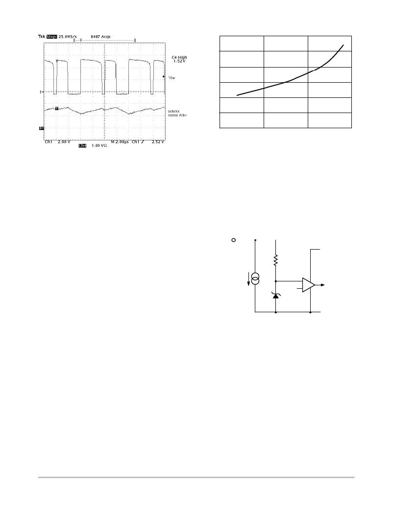
�SWITCHING� CURRENT� (A)�
�Figure� 8.� The� Regulator� in� Current� Limit�
�BOOST� Pin�
�The� BOOST� pin� provides� base� driving� current� for� the�
�power� switch.� A� voltage� higher� than� V� IN� provides� required�
�headroom� to� turn� on� the� power� switch.� This� in� turn� reduces�
�IC� power� dissipation� and� improves� overall� system�
�efficiency.� The� BOOST� pin� can� be� connected� to� an� external�
�boost� ?� strapping� circuit� which� typically� uses� a� 0.1� m� F� capacitor�
�and� a� 1N914� or� 1N4148� diode,� as� shown� in� Figure� 1.�
�When� the� power� switch� is� turned� on,� the� voltage� on� the�
�BOOST� pin� is� equal� to�
�Figure� 9.� The� Boost� Pin� Current� Includes� 7.0� mA�
�Pre� ?� Driver� Current� and� Base� Current� when� the�
�Switch� is� Turned� On.� The� Beta� Decline� of� the�
�Power� Switch� Further� Increases� the� Base�
�Current� at� High� Switching� Current�
�Shutdown�
�The� internal� power� switch� will� not� turn� on� until� the� V� IN�
�pin� rises� above� the� Startup� Voltage.� This� ensures� no�
�switching� will� occur� until� adequate� supply� voltage� is�
�provided� to� the� IC.� Refer� to� Figure� 10� for� the� SHDNB�
�(shutdown� ?� bar)� pin� input� circuit.�
�VBOOST� +� VIN� )� VO� *� VF�
�where:�
�V� F� =� diode� forward� voltage.�
�The� anode� of� the� diode� can� be� connected� to� any� DC�
�voltage� as� well� as� the� regulated� output� voltage� (Figure� 1).�
�However,� the� maximum� voltage� on� the� BOOST� pin� should�
�not� exceed� 40� V.�
�SHDNB�
�20k�
�±� 33%�
�1.2V�
�-�
�+�
�V� IN�
�As� shown� in� Figure� 9,� the� BOOST� pin� current� includes� a�
�constant� 7.0� mA� pre� ?� driver� current� and� base� current�
�proportional� to� switch� conducting� current.� A� detailed�
�V� Z� =� 6V� to� 8V�
�GND�
�discussion� of� this� current� is� conducted� in� Thermal�
�Consideration� section.� A� 0.1� m� F� capacitor� is� usually�
�adequate� for� maintaining� the� Boost� pin� voltage� during� the� on�
�time.�
�Figure� 10.�
�The� IC� enters� a� sleep� mode� when� the� SHDNB� pin� is� pulled�
�below� the� Shutdown� Threshold� Voltage.� In� sleep� mode,� the�
�power� switch� is� kept� open� and� the� supply� current� reduces� to�
�Shutdown� Quiescent� Current� (1� m� A� typically).� This� pin� has�
�an� internal� pull� ?� down� current.� When� not� in� use,� pull� this� pin�
�up� to� V� CC� with� a� resistor� (See� Figure� 1).� A� 100� k� W� pullup�
�resistor� will� ensure� safe� operation� from� below� 9� V� and�
�during� a� 40� V� load� dump� condition.�
�http://onsemi.com�
�8�
�相关PDF资料 |
PDF描述 |
|---|---|
| 345-072-521-204 | CARDEDGE 72POS DUAL .100 GREEN |
| ECC15DRES-S13 | CONN EDGECARD 30POS .100 EXTEND |
| XLN485 | RS485 CABLE |
| R1D-2415/HP | CONV DC/DC 1W 24VIN +/-15VOUT |
| ECC06DRTF | CONN EDGECARD 12POS DIP .100 SLD |
相关代理商/技术参数 |
参数描述 |
|---|---|
| NCV8843PWG | 功能描述:直流/直流开关转换器 1.5A LO VLT BUCK REG RoHS:否 制造商:STMicroelectronics 最大输入电压:4.5 V 开关频率:1.5 MHz 输出电压:4.6 V 输出电流:250 mA 输出端数量:2 最大工作温度:+ 85 C 安装风格:SMD/SMT |
| NCV8843PWR2G | 功能描述:直流/直流开关转换器 16L SOW EPAD RoHS:否 制造商:STMicroelectronics 最大输入电压:4.5 V 开关频率:1.5 MHz 输出电压:4.6 V 输出电流:250 mA 输出端数量:2 最大工作温度:+ 85 C 安装风格:SMD/SMT |
| NCV8851 | 制造商:ONSEMI 制造商全称:ON Semiconductor 功能描述:Automotive Grade Synchronous Buck Controller |
| NCV8851-1DBR2G | 制造商:ON Semiconductor 功能描述:SYNC BUCK CONTROLLER - Tape and Reel 制造商:ON Semiconductor 功能描述:SYNC BUCK CONTROLLER - Cut TR (SOS) 制造商:ON Semiconductor 功能描述:IC REG DL BCK/LINEAR 制造商:ON Semiconductor 功能描述:REEL / SYNC BUCK CONTROLLER |
| NCV8851-1GEVB | 制造商:ON Semiconductor 功能描述:NCV8851 -1 EVAL BD - Bulk 制造商:ON Semiconductor 功能描述:BOARD EVAL FOR NCV8851-1 |
发布紧急采购,3分钟左右您将得到回复。