参数资料
| 型号: | NE5230DG |
| 厂商: | ON Semiconductor |
| 文件页数: | 2/18页 |
| 文件大小: | 0K |
| 描述: | IC OPAMP LOW VOLTAGE 8-SOIC |
| 标准包装: | 98 |
| 放大器类型: | 通用 |
| 电路数: | 1 |
| 输出类型: | 满摆幅 |
| 转换速率: | 0.25 V/µs |
| 增益带宽积: | 600kHz |
| 电流 - 输入偏压: | 40nA |
| 电压 - 输入偏移: | 400µV |
| 电流 - 电源: | 1.1mA |
| 电流 - 输出 / 通道: | 32mA |
| 电压 - 电源,单路/双路(±): | 1.8 V ~ 15 V,±0.9 V ~ 7.5 V |
| 工作温度: | 0°C ~ 70°C |
| 安装类型: | 表面贴装 |
| 封装/外壳: | 8-SOIC(0.154",3.90mm 宽) |
| 供应商设备封装: | 8-SOICN |
| 包装: | 管件 |
NE5230, SA5230, SE5230
http://onsemi.com
10
REMOTE TRANSDUCER WITH CURRENT
TRANSMISSION
There are many ways to transmit information along two
wires, but current transmission is the most beneficial when
the sensing of remote signals is the aim. It is further
enhanced in the form of 4.0 to 20 mA information which is
used in many controltype systems. This method of
transmission provides immunity from line voltage drops,
large load resistance variations, and voltage noise pickup.
The zero reference of 4mA not only can show if there is a
break in the line when no current is flowing, but also can
power the transducer at the remote location. Usually the
transducer itself is not equipped to provide for the current
transmission. The unique features of the NE5230 can
provide high output current capability coupled with low
power consumption. It can be remotely connected to the
transducer to create a current loop with minimal external
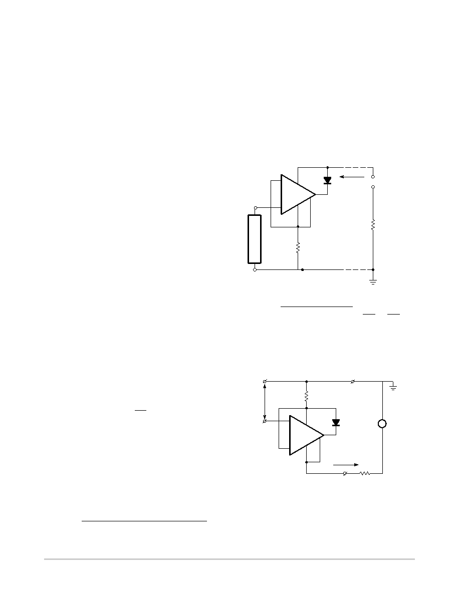
components. The circuits for this are shown in Figures 6
and 7. Here, the part is configured as a voltagetocurrent,
or transconductance amplifier. This is a novel circuit that
takes advantage of the NE5230’s large openloop gain. In
AC applications, the load current will decrease as the
openloop gain rolls off in magnitude. The low offset
voltage and current sinking capabilities of the NE5230 must
also be considered in this application.
The NE5230 circuit shown in Figure 6 is a pseudo
transistor configuration. The inverting input is equivalent to
the “base,” the point where VEE and the noninverting input
meet is the “emitter,” and the connection after the output
diode meets the VCC pin is the collector. The output diode
is essential to keep the output from saturating in this
configuration. From here it can be seen that the base and
emitter form a voltagefollower and the voltage present at
RC must equal the input voltage present at the inverting
input. Also, the emitter and collector form a
currentfollower and the current flowing through RC is
equivalent to the current through RL and the amplifier. This
sets up the current loop. Therefore, the following equation
can be formulated for the working current transmission line.
The load current is:
IL +
VIN
RC
(eq. 2)
and proportional to the input voltage for a set RC. Also, the
current is constant no matter what load resistance is used
while within the operating bandwidth range of the op amp.
When the NE5230’s supply voltage falls past a certain point,
the current cannot remain constant. This is the “voltage
compliance” and is very good for this application because of
the near rail output voltage. The equation that determines the
voltage compliance as well as the largest possible load
resistor for the NE5230 is as follows:
RLmax +
Vremote supply * VCC min * VIN max
IL
(eq. 3)
Where VCC min is the worstcase power supply voltage
(approximately 1.8 V) that will still keep the part
operational. As an example, when using a 15 V remote
power supply, a current sensing resistor of 1.0
W, and an
input voltage (VIN) of 20 mV, the output current (IL) is
20 mA. Furthermore, a load resistance of zero to
approximately 650
W can be inserted in the loop without any
change in current when the bias currentcontrol pin is tied
to the negative supply pin. The voltage drop across the load
and line resistance will not affect the NE5230 because it will
operate down to 1.8 V. With a 15 V remote supply, the
voltage available at the amplifier is still enough to power it
with the maximum 20 mA output into the 650
W load.
Figure 6. The NE5230 as a Remote Transducer
Transconductance Amp with 4.0 20 mA Current
Transmission Output Capability
T
R
A
N
S
D
U
C
E
R
V
REMOTE
POWER
SUPPLY
NE5230
VCC
VEE
VIN
IOUT
3
2
4
5
6
7
+
RC
RL
+
NOTES:
1. IOUT = VIN/RC
2. RL MAX ≈
VREMOTE * 1.8V * VINMAX
IOUT
For RC = 1.0 W
IOUT
4mA
VIN
4mV
20mA
20mV
Figure 7. The Same Type of Circuit as Figure 6, but
for Sourcing Current to the Load
VCC
NE5230
3
2
4
5
6
7
+
VEE
+ IOUT
+
VIN
RC
RL
VCC
+
相关PDF资料 |
PDF描述 |
|---|---|
| MC33074ADTBG | IC OPAMP QUAD 4.5MHZ 14TSSOP |
| 951135-2530-AR-TP | CONN HEADER 35POS 2MM VERT SMD |
| MC33074ADTB | IC OPAMP QUAD 4.5MHZ 14TSSOP |
| 951133-2530-AR-PT | CONN HEADER 33POS 2MM VERT SMD |
| CRCW04026R19FKED | RES 6.19 OHM 1/16W 1% 0402 SMD |
相关代理商/技术参数 |
参数描述 |
|---|---|
| NE5230DR2 | 功能描述:运算放大器 - 运放 1.8V Single Rail to RoHS:否 制造商:STMicroelectronics 通道数量:4 共模抑制比(最小值):63 dB 输入补偿电压:1 mV 输入偏流(最大值):10 pA 工作电源电压:2.7 V to 5.5 V 安装风格:SMD/SMT 封装 / 箱体:QFN-16 转换速度:0.89 V/us 关闭:No 输出电流:55 mA 最大工作温度:+ 125 C 封装:Reel |
| NE5230DR2G | 功能描述:运算放大器 - 运放 1.8V Single Rail to Rail Commercial Temp RoHS:否 制造商:STMicroelectronics 通道数量:4 共模抑制比(最小值):63 dB 输入补偿电压:1 mV 输入偏流(最大值):10 pA 工作电源电压:2.7 V to 5.5 V 安装风格:SMD/SMT 封装 / 箱体:QFN-16 转换速度:0.89 V/us 关闭:No 输出电流:55 mA 最大工作温度:+ 125 C 封装:Reel |
| NE5230N | 功能描述:运算放大器 - 运放 1.8V Single Rail to RoHS:否 制造商:STMicroelectronics 通道数量:4 共模抑制比(最小值):63 dB 输入补偿电压:1 mV 输入偏流(最大值):10 pA 工作电源电压:2.7 V to 5.5 V 安装风格:SMD/SMT 封装 / 箱体:QFN-16 转换速度:0.89 V/us 关闭:No 输出电流:55 mA 最大工作温度:+ 125 C 封装:Reel |
| NE5230NG | 功能描述:运算放大器 - 运放 1.8V Single Rail to Rail Commercial Temp RoHS:否 制造商:STMicroelectronics 通道数量:4 共模抑制比(最小值):63 dB 输入补偿电压:1 mV 输入偏流(最大值):10 pA 工作电源电压:2.7 V to 5.5 V 安装风格:SMD/SMT 封装 / 箱体:QFN-16 转换速度:0.89 V/us 关闭:No 输出电流:55 mA 最大工作温度:+ 125 C 封装:Reel |
| NE5232 | 制造商:PHILIPS 制造商全称:NXP Semiconductors 功能描述:Matched dual high-performance low-voltage operational amplifier |
发布紧急采购,3分钟左右您将得到回复。