参数资料
| 型号: | NIS1050MNTBG |
| 厂商: | ON Semiconductor |
| 文件页数: | 4/5页 |
| 文件大小: | 0K |
| 描述: | IC PWR INTERFACE PROTECT 6-WDFN |
| 标准包装: | 1 |
| 应用: | 移动通信 |
| 电源电压: | 3 V ~ 30 V |
| 封装/外壳: | 6-WDFN 裸露焊盘 |
| 供应商设备封装: | 6-WDFN(2x2) |
| 包装: | 标准包装 |
| 安装类型: | 表面贴装 |
| 其它名称: | NIS1050MNTBGOSDKR |
NIS1050
http://onsemi.com
4
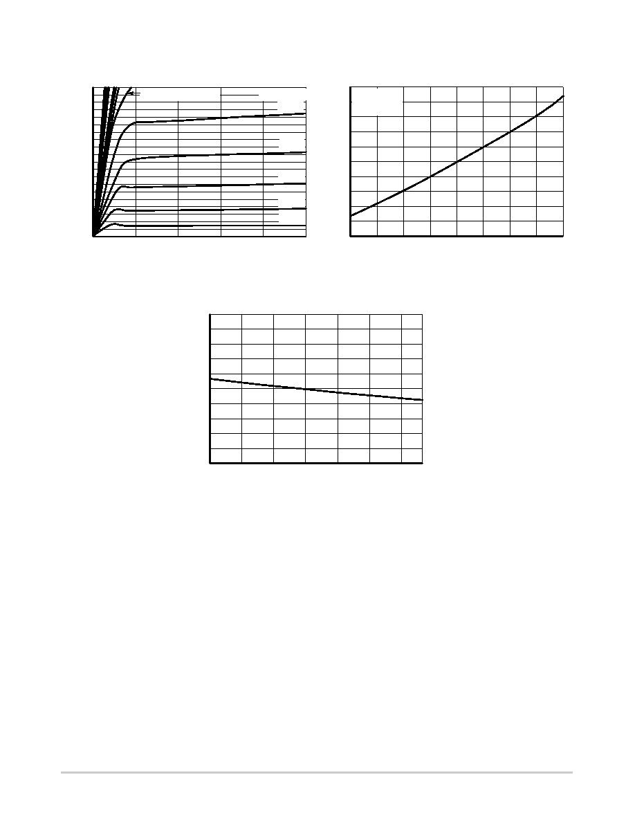
TYPICAL PERFORMANCE CURVES
1.6
1.2
1.4
1.0
0.8
0.6
05
2
1
VDS, DRAINTOSOURCE VOLTAGE (VOLTS)
I D
,DRAIN
CURRENT
(AMPS)
0
Figure 4. OnRegion Characteristics
Figure 5. OnResistance Variation with
Temperature
Figure 6. Output Voltage Variation with
Temperature
TJ, JUNCTION TEMPERATURE (°C)
R
DS(on)
,DRAIN
TO
SOURCE
RESIST
ANCE
(NORMALIZED)
5
50
25
0
25
75
125
100
3
1
2
ID = 2 A
VGS = 4.5 V
3
VGS = 1.7 V to 8 V
1.5 V
4
150
1.6 V
1.4 V
1.3 V
1.2 V
TJ = 25°C
TJ, JUNCTION TEMPERATURE (°C)
110
85
60
35
10
15
40
4.80
4.85
4.90
4.95
5.00
5.15
5.20
5.30
V
out
,OUTPUT
VOL
TAGE
(V)
5.05
5.10
5.25
Mounting Considerations
The LDO and MOSFET are both attached to thermal pads
to provide a low impedance path for the heat generated in
these devices. Both of these pads should have a solid
connection to as much board copper area as possible in order
to maintain a low operating temperature. The main purpose
of both of these pads is for thermal connections, not
electrical connections.
Pad 7 is the input voltage for the LDO. It is electrically
connected to the Vcc pin. This connection is optional and
will have a negligible difference in the electrical
performance of the chip due to the current into the LDO.
Pad 8 is the drain of the power MOSFET. This pad will
also have a low electrical impedance. Either pad 8, pad 6 or
both may be used for electrical connections. The total
impedance of the FET will not vary significantly since pad
6 is part of the lead-frame and therefore connected to pad 8
by a metal path on the lead frame. The majority of the
package impedance comes from the resistance between the
source and pin 1, since this is connected by bond wires.
Bypass Capacitors
The LDO has been designed to operate in a stable mode
without bypass capacitors; however, it is recommended to
use a low ESR capacitor if fast, ac transients or other
switching type currents will be present. Typically, a value of
1 to 10 nF is adequate for an output bypass capacitor. A 1 nF
capacitor may be added to the input if the input source is
noisy or if it has a high ac impedance due to long trace
lengths.
相关PDF资料 |
PDF描述 |
|---|---|
| NL7WB66US | IC SWITCH DUAL SPST US8 |
| NLAS1053US | IC SWITCH SPDT US8 |
| NLAS2066UST3 | IC SWITCH DUAL SPST US8 |
| NLAS3158MNR2G | IC SWITCH DUAL SPDT 12DFN |
| NLAS323US | IC SWITCH DUAL SPST US8 |
相关代理商/技术参数 |
参数描述 |
|---|---|
| NIS3001 | 制造商:ONSEMI 制造商全称:ON Semiconductor 功能描述:Integrated Driver and MOSFET Power Chip for Synchronous Buck Controllers |
| NIS3001/D | 制造商:ONSEMI 制造商全称:ON Semiconductor 功能描述:Integrated Drive and MOSFET Power Chip for Synchronous Buck Controllers |
| NIS3001A/D | 制造商:未知厂家 制造商全称:未知厂家 功能描述:Integrated Drive and MOSFET Power Chip for Synchronous Buck Controllers |
| NIS3001QPT1 | 制造商:ONSEMI 制造商全称:ON Semiconductor 功能描述:Integrated Driver and MOSFET Power Chip for Synchronous Buck Controllers |
| NIS5101 | 制造商:ONSEMI 制造商全称:ON Semiconductor 功能描述:SMART HotPlug IC/Inrush Limiter/Circuit Breaker |
发布紧急采购,3分钟左右您将得到回复。