参数资料
| 型号: | NL17SHT08P5T5G |
| 厂商: | ON Semiconductor |
| 文件页数: | 1/5页 |
| 文件大小: | 0K |
| 描述: | IC GATE AND SGL 2INPUT SOT953 |
| 标准包装: | 8,000 |
| 逻辑类型: | 与门 |
| 电路数: | 1 |
| 输入数: | 2 |
| 电源电压: | 3 V ~ 5.5 V |
| 电流 - 静态(最大值): | 1µA |
| 输出电流高,低: | 8mA,8mA |
| 逻辑电平 - 低: | 0.53 V ~ 0.8 V |
| 逻辑电平 - 高: | 1.4 V ~ 2 V |
| 额定电压和最大 CL 时的最大传播延迟: | 7.9ns @ 4.5V ~ 5.5V,50pF |
| 工作温度: | -55°C ~ 125°C |
| 安装类型: | 表面贴装 |
| 供应商设备封装: | SOT-953 |
| 封装/外壳: | SOT-953 |
| 包装: | 带卷 (TR) |
Semiconductor Components Industries, LLC, 2011
August, 2011 Rev. 0
1
Publication Order Number:
NL17SHT08/D
NL17SHT08
2-Input AND Gate /
CMOS Logic Level Shifter
The NL17SHT08 is an advanced high speed CMOS 2input AND
gate fabricated with silicon gate CMOS technology. It achieves high
speed operation similar to equivalent Bipolar Schottky TTL while
maintaining CMOS low power dissipation.
The internal circuit is composed of three stages, including a buffer
output which provides high noise immunity and stable output.
The device input is compatible with TTLtype input thresholds and
the output has a full 5 V CMOS level output swing. The input protection
circuitry on this device allows overvoltage tolerance on the input,
allowing the device to be used as a logiclevel translator from 3 V
CMOS logic to 5 V CMOS Logic or from 1.8 V CMOS logic to 3 V
CMOS Logic while operating at the highvoltage power supply.
The NL17SHT08 input structure provides protection when voltages
up to 7 V are applied, regardless of the supply voltage. This allows the
NL17SHT08 to be used to interface 5 V circuits to 3 V circuits. The
output structures also provide protection when VCC = 0 V. These input
and output structures help prevent device destruction caused by supply
voltage input/output voltage mismatch, battery backup, hot
insertion, etc.
Features
High Speed: tPD = 3.5 ns (Typ) at VCC = 5 V
Low Power Dissipation: ICC = 1 mA (Max) at TA = 25°C
TTLCompatible Inputs: VIL = 0.8 V; VIH = 2 V
CMOSCompatible Outputs: VOH > 0.8 VCC; VOL < 0.1 VCC @Load
Power Down Protection Provided on Inputs and Outputs
Balanced Propagation Delays
Pin and Function Compatible with Other Standard Logic Families
These are PbFree Devices
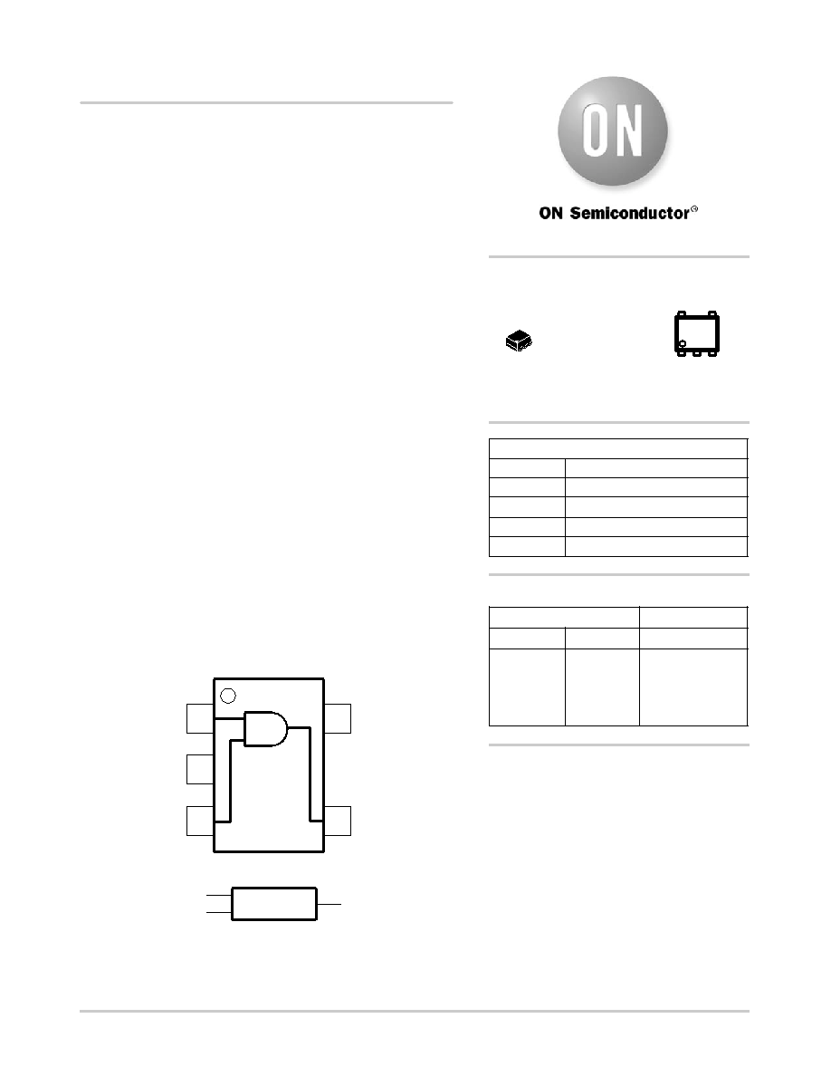
VCC
IN B
IN A
OUT Y
GND
IN A
IN B
OUT Y
&
Figure 1. Pinout (Top View)
Figure 2. Logic Symbol
1
2
34
5
PIN ASSIGNMENT
1
2
3IN B
IN A
GND
4
5VCC
OUT Y
L
H
L
H
L
H
FUNCTION TABLE
Inputs
Output
AB
L
H
Y
See detailed ordering and shipping information in the package
dimensions section on page 4 of this data sheet.
ORDERING INFORMATION
MARKING
DIAGRAM
http://onsemi.com
SOT953
CASE 527AE
P
= Specific Device Code
M
= Month Code
PM
1
相关PDF资料 |
PDF描述 |
|---|---|
| NL17SHT32P5T5G | IC GATE OR SGL 2INPUT SOT953 |
| NL17SV08XV5T2 | IC GATE AND SGL LV 2INP SOT553 |
| NL17SZ00XV5T2 | IC GATE NAND SINGLE 2INP SOT553 |
| NL17SZ02XV5T2 | IC GATE NOR SINGLE 2INPUT SOT553 |
| NL17SZ04XV5T2 | IC INVERTER SINGLE SOT553 |
相关代理商/技术参数 |
参数描述 |
|---|---|
| NL17SHT126P5T5G | 功能描述:缓冲器和线路驱动器 NON-INVERTING 3- STATE BUF RoHS:否 制造商:Micrel 输入线路数量:1 输出线路数量:2 极性:Non-Inverting 电源电压-最大:+/- 5.5 V 电源电压-最小:+/- 2.37 V 最大工作温度:+ 85 C 安装风格:SMD/SMT 封装 / 箱体:MSOP-8 封装:Reel |
| NL17SHT32P5T5G | 功能描述:逻辑门 SINGLE 2-INPUT OR GATE RoHS:否 制造商:Texas Instruments 产品:OR 逻辑系列:LVC 栅极数量:2 线路数量(输入/输出):2 / 1 高电平输出电流:- 16 mA 低电平输出电流:16 mA 传播延迟时间:3.8 ns 电源电压-最大:5.5 V 电源电压-最小:1.65 V 最大工作温度:+ 125 C 安装风格:SMD/SMT 封装 / 箱体:DCU-8 封装:Reel |
| NL17SV00 | 制造商:ONSEMI 制造商全称:ON Semiconductor 功能描述:Single 2-Input NAND Gate |
| NL17SV00XV5T2 | 功能描述:IC GATE NAND SGL 2INPUT SOT-553 RoHS:否 类别:集成电路 (IC) >> 逻辑 - 栅极和逆变器 系列:17SV 标准包装:1 系列:74ACTQ 逻辑类型:与非门 电路数:3 输入数:3 特点:- 电源电压:4.5 V ~ 5.5 V 电流 - 静态(最大值):2µA 输出电流高,低:24mA,24mA 逻辑电平 - 低:0.8V 逻辑电平 - 高:2V 额定电压和最大 CL 时的最大传播延迟:7.5ns @ 5V,50pF 工作温度:-40°C ~ 85°C 安装类型:表面贴装 供应商设备封装:14-SOIC 封装/外壳:14-SOIC(0.154",3.90mm 宽) 包装:管件 其它名称:74ACTQ10SCCT74ACTQ10SCCT-ND |
| NL17SV00XV5T2G | 功能描述:逻辑门 ULTRA LOW VOL2 INPUT LOG RoHS:否 制造商:Texas Instruments 产品:OR 逻辑系列:LVC 栅极数量:2 线路数量(输入/输出):2 / 1 高电平输出电流:- 16 mA 低电平输出电流:16 mA 传播延迟时间:3.8 ns 电源电压-最大:5.5 V 电源电压-最小:1.65 V 最大工作温度:+ 125 C 安装风格:SMD/SMT 封装 / 箱体:DCU-8 封装:Reel |
发布紧急采购,3分钟左右您将得到回复。