参数资料
| 型号: | NL37WZ07USG |
| 厂商: | ON Semiconductor |
| 文件页数: | 2/5页 |
| 文件大小: | 0K |
| 描述: | IC GATE INVERTER TRIPLE 1IN US8 |
| 标准包装: | 1 |
| 系列: | 37WZ |
| 逻辑类型: | 缓冲器/线路驱动器,非反相并带开漏极 |
| 元件数: | 3 |
| 每个元件的位元数: | 1 |
| 输出电流高,低: | -,32mA |
| 电源电压: | 1.65 V ~ 5.5 V |
| 工作温度: | -55°C ~ 125°C |
| 安装类型: | 表面贴装 |
| 封装/外壳: | 8-VFSOP(0.091",2.30mm 宽) |
| 供应商设备封装: | US8 |
| 包装: | 标准包装 |
| 其它名称: | NL37WZ07USGOSDKR |
NL37WZ07
http://onsemi.com
2
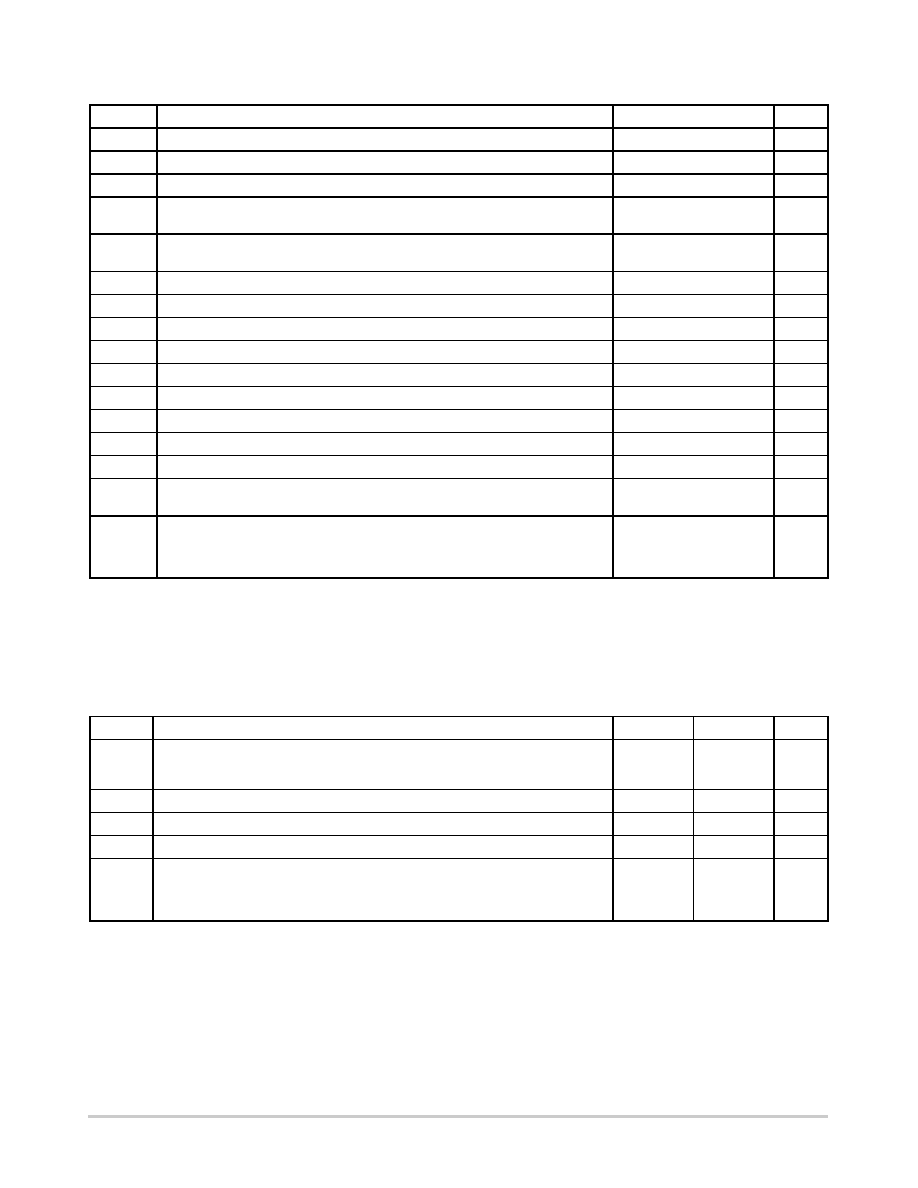
MAXIMUM RATINGS
Symbol
Parameter
Value
Units
VCC
DC Supply Voltage
0.5 to +7.0
V
VI
DC Input Voltage
0.5 to +7.0
V
VO
DC Output Voltage
0.5 to +7.0
V
IIK
DC Input Diode Current
VI < GND
50
mA
IOK
DC Output Diode Current
VO < GND
50
mA
IO
DC Output Sink Current
±50
mA
ICC
DC Supply Current per Supply Pin
±100
mA
IGND
DC Ground Current per Ground Pin
±100
mA
TSTG
Storage Temperature Range
65 to +150
°C
TL
Lead Temperature, 1 mm from Case for 10 Seconds
260
°C
TJ
Junction Temperature under Bias
+150
°C
qJA
Thermal Resistance (Note 1)
250
°C/W
PD
Power Dissipation in Still Air at 85°C
250
mW
MSL
Moisture Sensitivity
Level 1
FR
Flammability Rating
Oxygen Index: 28 to 34
UL 94 V0 @ 0.125 in
VESD
ESD Withstand Voltage
Human Body Model (Note 2)
Machine Model (Note 3)
Charged Device Model (Note 4)
> 2000
> 150
N/A
V
Stresses exceeding Maximum Ratings may damage the device. Maximum Ratings are stress ratings only. Functional operation above the
Recommended Operating Conditions is not implied. Extended exposure to stresses above the Recommended Operating Conditions may affect
device reliability.
1. Measured with minimum pad spacing on an FR4 board, using 10 mmby1 inch, 2ounce copper trace with no air flow.
2. Tested to EIA/JESD22A114A.
3. Tested to EIA/JESD22A115A.
4. Tested to JESD22C101A.
RECOMMENDED OPERATING CONDITIONS
Symbol
Parameter
Min
Max
Units
VCC
Supply Voltage
Operating
Data Retention Only
1.65
1.5
5.5
V
VI
Input Voltage (Note 5)
0
5.5
V
VO
Output Voltage (HIGH or LOW State)
0
5.5
V
TA
Operating FreeAir Temperature
55
+125
°C
Dt/DV
Input Transition Rise or Fall Rate
VCC = 2.5 V ±0.2 V
VCC = 3.0 V ±0.3 V
VCC = 5.0 V ±0.5 V
0
20
10
5
ns/V
5. Unused inputs may not be left open. All inputs must be tied to a high or lowlogic input voltage level.
相关PDF资料 |
PDF描述 |
|---|---|
| NL37WZ17USG | IC BUFF SCHM TRG TRPL N-INV US8 |
| CD4072BNSRG4 | IC DUAL 4INPUT OR GATE 14-SOP |
| CD4071BNSRG4 | IC QUAD 2INPUT OR GATE 14-SOP |
| EDSTLZ950/9 | TERM BLOCK HDR 5.08MM 9POS PCB |
| EDSTLZ955/9 | TERM BLOCK HDR 5.08MM 9POS PCB |
相关代理商/技术参数 |
参数描述 |
|---|---|
| NL37WZ07USG-CUT TAPE | 制造商:ON 功能描述:NL37WZ07 Series 1.65 to 5.5 V Triple Buffer w/Open Drain - US-8 |
| NL37WZ14 | 制造商:ONSEMI 制造商全称:ON Semiconductor 功能描述:Triple Schmitt-Trigger Inverter |
| NL37WZ14/D | 制造商:ONSEMI 制造商全称:ON Semiconductor 功能描述:Triple Schmitt-Trigger Inverter |
| NL37WZ14_06 | 制造商:ONSEMI 制造商全称:ON Semiconductor 功能描述:Triple Schmitt−Trigger Inverter |
| NL37WZ14US | 功能描述:变换器 1.65-5.5V CMOS Dual RoHS:否 制造商:NXP Semiconductors 电路数量:6 逻辑系列:74ABT 逻辑类型:BiCMOS 高电平输出电流:- 15 mA 低电平输出电流:20 mA 传播延迟时间:2.2 ns 电源电压-最大:5.5 V 电源电压-最小:4.5 V 最大工作温度:+ 85 C 最小工作温度:- 40 C 工作温度范围: 封装 / 箱体:DIP-14 封装:Tube |
发布紧急采购,3分钟左右您将得到回复。