参数资料
| 型号: | NL37WZ14US |
| 厂商: | ON Semiconductor |
| 文件页数: | 2/5页 |
| 文件大小: | 0K |
| 描述: | IC INVERTER TRPL OPEN DRAIN US8 |
| 产品变化通告: | Product Discontinuation 20/Aug/2008 |
| 标准包装: | 1 |
| 系列: | 37WZ |
| 逻辑类型: | 逆变器,缓冲器 |
| 电路数: | 3 |
| 输入数: | 1 |
| 特点: | 施密特触发器 |
| 电源电压: | 1.65 V ~ 5.5 V |
| 电流 - 静态(最大值): | 1µA |
| 输出电流高,低: | 32mA,32mA |
| 逻辑电平 - 低: | 0.4 V ~ 1.2 V |
| 逻辑电平 - 高: | 1.8 V ~ 3.6 V |
| 额定电压和最大 CL 时的最大传播延迟: | 4.9ns @ 5V,50pF |
| 工作温度: | -55°C ~ 125°C |
| 安装类型: | 表面贴装 |
| 供应商设备封装: | US8 |
| 封装/外壳: | 8-VFSOP(0.091",2.30mm 宽) |
| 包装: | 剪切带 (CT) |
| 其它名称: | NL37WZ14USOSCT |
NL37WZ14
http://onsemi.com
2
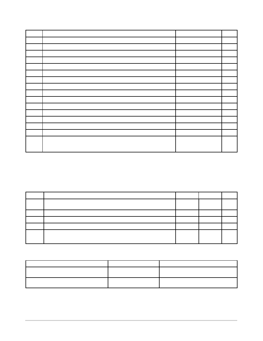
MAXIMUM RATINGS
Symbol
Parameter
Value
Unit
VCC
DC Supply Voltage
*0.5 to )7.0
V
VI
DC Input Voltage
*0.5 to )7.0
V
VO
DC Output Voltage
*0.5 to )7.0
V
IIK
DC Input Diode Current
VI < GND
*50
mA
IOK
DC Output Diode Current
VO < GND
*50
mA
IO
DC Output Sink Current
$50
mA
ICC
DC Supply Current per Supply Pin
$100
mA
IGND
DC Ground Current per Ground Pin
$100
mA
TSTG
Storage Temperature Range
*65 to )150
_C
TL
Lead Temperature, 1 mm from Case for 10 Seconds
260
_C
TJ
Junction Temperature under Bias
)150
_C
qJA
Thermal Resistance (Note 1)
250
_C/W
PD
Power Dissipation in Still Air at 85_C
250
mW
MSL
Moisture Sensitivity
Level 1
FR
Flammability Rating
Oxygen Index: 28 to 34
UL 94 V0 @ 0.125 in
VESD
ESD Withstand Voltage
Human Body Model (Note 2)
Machine Model (Note 3)
Charged Device Model (Note 4)
> 2000
> 200
N/A
V
Stresses exceeding Maximum Ratings may damage the device. Maximum Ratings are stress ratings only. Functional operation above the
Recommended Operating Conditions is not implied. Extended exposure to stresses above the Recommended Operating Conditions may affect
device reliability.
1. Measured with minimum pad spacing on an FR4 board, using 10 mmby1 inch, 2ounce copper trace with no air flow.
2. Tested to EIA/JESD22A114A.
3. Tested to EIA/JESD22A115A.
4. Tested to JESD22C101A.
RECOMMENDED OPERATING CONDITIONS
Symbol
Parameter
Min
Max
Unit
VCC
Supply Voltage
Operating
Data Retention Only
2.3
1.5
5.5
V
VI
Input Voltage
(Note 5)
0
5.5
V
VO
Output Voltage
(HIGH or LOW State)
0
5.5
V
TA
Operating FreeAir Temperature
*55
)125
_C
Dt/DV
Input Transition Rise or Fall Rate
VCC = 2.5 V $0.2 V
VCC = 3.0 V $0.3 V
VCC = 5.0 V $0.5 V
0
No Limit
ns/V
5. Unused inputs may not be left open. All inputs must be tied to a high or lowlogic input voltage level.
DEVICE ORDERING INFORMATION
Device Order Number
Package
Shipping
NL37WZ14USG
US8
(PbFree)
3000 / Tape & Reel
NLV37WZ14USG*
US8
(PbFree)
3000 / Tape & Reel
For information on tape and reel specifications, including part orientation and tape sizes, please refer to our Tape and Reel Packaging
Specifications Brochure, BRD8011/D.
*NLV Prefix for Automotive and Other Applications Requiring Unique Site and Control Change Requirements; AECQ100 Qualified and PPAP
Capable.
相关PDF资料 |
PDF描述 |
|---|---|
| NL7SZ58DFT2G | IC GATE MULTIFUNCT CONF SC-88 |
| NL7SZ98DFT2G | IC GATE MULTIFUNCT CONF SC-88 |
| NLSF302MNR2 | IC GATE NOR QUAD CMOS 2INP 16QFN |
| NLSF308MNR2 | IC GATE AND QUAD CMOS 2INP 16QFN |
| NLU1G00BMX1TCG | IC GATE NAND SGL 2INPUT 6ULLGA |
相关代理商/技术参数 |
参数描述 |
|---|---|
| NL37WZ14USG | 功能描述:变换器 1.65-5.5V CMOS Dual Triple Schmitt RoHS:否 制造商:NXP Semiconductors 电路数量:6 逻辑系列:74ABT 逻辑类型:BiCMOS 高电平输出电流:- 15 mA 低电平输出电流:20 mA 传播延迟时间:2.2 ns 电源电压-最大:5.5 V 电源电压-最小:4.5 V 最大工作温度:+ 85 C 最小工作温度:- 40 C 工作温度范围: 封装 / 箱体:DIP-14 封装:Tube |
| NL37WZ14USG-CUT TAPE | 制造商:ON 功能描述:NL37WZ14 Series 1.65 to 5.5 V Triple Inverter Schmitt - US-8 |
| NL37WZ16 | 制造商:ONSEMI 制造商全称:ON Semiconductor 功能描述:Triple Buffer |
| NL37WZ16/D | 制造商:未知厂家 制造商全称:未知厂家 功能描述:Triple Buffer |
| NL37WZ16_06 | 制造商:ONSEMI 制造商全称:ON Semiconductor 功能描述:Triple Buffer |
发布紧急采购,3分钟左右您将得到回复。