- 您现在的位置:买卖IC网 > PDF目录17982 > NTB6410ANT4G (ON Semiconductor)MOSFET N-CH 100V 76A D2PAK PDF资料下载
参数资料
| 型号: | NTB6410ANT4G |
| 厂商: | ON Semiconductor |
| 文件页数: | 1/7页 |
| 文件大小: | 0K |
| 描述: | MOSFET N-CH 100V 76A D2PAK |
| 标准包装: | 800 |
| FET 型: | MOSFET N 通道,金属氧化物 |
| FET 特点: | 标准 |
| 漏极至源极电压(Vdss): | 100V |
| 电流 - 连续漏极(Id) @ 25° C: | 76A |
| 开态Rds(最大)@ Id, Vgs @ 25° C: | 13 毫欧 @ 76A,10V |
| Id 时的 Vgs(th)(最大): | 4V @ 250µA |
| 闸电荷(Qg) @ Vgs: | 120nC @ 10V |
| 输入电容 (Ciss) @ Vds: | 4500pF @ 25V |
| 功率 - 最大: | 188W |
| 安装类型: | 表面贴装 |
| 封装/外壳: | TO-263-3,D²Pak(2 引线+接片),TO-263AB |
| 供应商设备封装: | D2PAK |
| 包装: | 带卷 (TR) |
�� �
�
�NTB6410AN,� NTP6410AN,�
�NVB6410AN�
�N-Channel� Power� MOSFET�
�100� V,� 76� A,� 13� m� W�
�Features�
�?� Low� R� DS(on)�
�?� High� Current� Capability�
�?� 100%� Avalanche� Tested�
�?� NVB� Prefix� for� Automotive� and� Other� Applications� Requiring�
�Unique� Site� and� Control� Change� Requirements;� AEC� ?� Q101�
�Qualified� and� PPAP� Capable�
�?�
�These� Devices� are� Pb� ?� Free� and� are� RoHS� Compliant�
�V� (BR)DSS�
�100� V�
�http://onsemi.com�
�R� DS(ON)� MAX�
�13� m� W� @� 10� V�
�N� ?� Channel�
�I� D� MAX�
�(Note� 1)�
�76� A�
�D�
�MAXIMUM� RATINGS� (T� J� =� 25� °� C� Unless� otherwise� specified)�
�Parameter�
�Symbol�
�Value�
�Unit�
�Drain� ?� to� ?� Source� Voltage�
�Gate� ?� to� ?� Source� Voltage� ?� Continuous�
�V� DSS�
�V� GS�
�100�
�$� 20�
�V�
�V�
�G�
�Continuous� Drain�
�Current� R� q� JC�
�Power� Dissipation�
�R� q� JC�
�Steady�
�State�
�Steady�
�State�
�T� C� =� 25� °� C�
�T� C� =� 100� °� C�
�T� C� =� 25� °� C�
�I� D�
�P� D�
�76�
�54�
�188�
�A�
�W�
�4�
�S�
�4�
�Pulsed� Drain� Current�
�t� p� =� 10� m� s�
�I� DM�
�305�
�A�
�1�
�2�
�Operating� Junction� and� Storage� Temperature�
�Range�
�T� J� ,� T� stg�
�?� 55� to�
�+175�
�°� C�
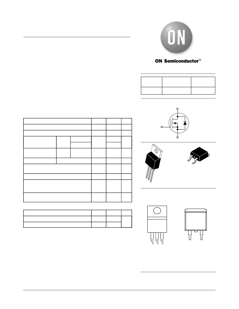
�TO� ?� 220AB�
�3�
�D� 2� PAK�
�Drain�
�Source� Current� (Body� Diode)�
�Single� Pulse� Drain� ?� to� ?� Source� Avalanche�
�Energy� (V� DD� =� 50� Vdc,� V� GS� =� 10� Vdc,�
�I� L(pk)� =� 57.7� A,� L� =� 0.3� mH,� R� G� =� 25� W� )�
�Lead� Temperature� for� Soldering�
�Purposes,� 1/8� ″� from� Case� for� 10� Seconds�
�THERMAL� RESISTANCE� RATINGS�
�I� S�
�E� AS�
�T� L�
�76�
�500�
�260�
�A�
�mJ�
�°� C�
�1�
�2�
�3�
�4�
�CASE� 221A� CASE� 418B�
�STYLE� 5� STYLE� 2�
�MARKING� DIAGRAM�
�&� PIN� ASSIGNMENT�
�4�
�Drain�
�Parameter�
�Symbol�
�Max�
�Unit�
�3�
�1�
�3�
�Source�
�Gate�
�Source�
�Junction� ?� to� ?� Case� (Drain)� Steady� State� R� q� JC� 0.8� °� C/W�
�Junction� ?� to� ?� Ambient� (Note� 1)� R� q� JA� 32�
�Stresses� exceeding� Maximum� Ratings� may� damage� the� device.� Maximum�
�Ratings� are� stress� ratings� only.� Functional� operation� above� the� Recommended�
�Operating� Conditions� is� not� implied.� Extended� exposure� to� stresses� above� the�
�Recommended� Operating� Conditions� may� affect� device� reliability.�
�1.� Surface� mounted� on� FR4� board� using� 1� sq� in� pad� size,�
�(Cu� Area� 1.127� sq� in� [2� oz]� including� traces).�
�1�
�Gate�
�NTP�
�6410ANG�
�AYWW�
�2�
�Drain�
�NTB�
�6410ANG�
�AYWW�
�2�
�Drain�
�6410AN� =� Specific� Device� Code�
�G� =� Pb� ?� Free� Device�
�A� =� Assembly� Location�
�Y� =� Year�
�WW� =� Work� Week�
�ORDERING� INFORMATION�
�See� detailed� ordering� and� shipping� information� in� the� package�
�dimensions� section� on� page� 5� of� this� data� sheet.�
�?� Semiconductor� Components� Industries,� LLC,� 2012�
�January,� 2012� ?� Rev.� 1�
�1�
�Publication� Order� Number:�
�NTB6410AN/D�
�相关PDF资料 |
PDF描述 |
|---|---|
| MC18FD301J-F | CAP MICA 300PF 500V 5% 1812 |
| CD5EC330GO3F | CAP MICA 33PF 300V 2% RADIAL |
| CD10ED500GO3F | CAP MICA 50PF 500V 2% RADIAL |
| CD15FC561JO3F | CAP MICA 560PF 300V 5% RADIAL |
| CD15FC561JO3 | CAP MICA 560PF 300V 5% RADIAL |
相关代理商/技术参数 |
参数描述 |
|---|---|
| NTB6411AN | 制造商:ONSEMI 制造商全称:ON Semiconductor 功能描述:N-Channel Power MOSFET 100 V, 72 A, 14 mΩ |
| NTB6411ANG | 功能描述:MOSFET NFET D2PAK 100V 72A 14MO RoHS:否 制造商:STMicroelectronics 晶体管极性:N-Channel 汲极/源极击穿电压:650 V 闸/源击穿电压:25 V 漏极连续电流:130 A 电阻汲极/源极 RDS(导通):0.014 Ohms 配置:Single 最大工作温度: 安装风格:Through Hole 封装 / 箱体:Max247 封装:Tube |
| NTB6411ANT4G | 功能描述:MOSFET NFET D2PAK 100V 75A 16MO RoHS:否 制造商:STMicroelectronics 晶体管极性:N-Channel 汲极/源极击穿电压:650 V 闸/源击穿电压:25 V 漏极连续电流:130 A 电阻汲极/源极 RDS(导通):0.014 Ohms 配置:Single 最大工作温度: 安装风格:Through Hole 封装 / 箱体:Max247 封装:Tube |
| NTB6412AN | 制造商:ONSEMI 制造商全称:ON Semiconductor 功能描述:N-Channel Power MOSFET 100 V, 58 A, 18.2 mΩ |
| NTB6412AN_12 | 制造商:ONSEMI 制造商全称:ON Semiconductor 功能描述:N-Channel Power MOSFET |
发布紧急采购,3分钟左右您将得到回复。