- 您现在的位置:买卖IC网 > PDF目录17500 > NTB65N02RT4 (ON Semiconductor)MOSFET N-CH 25V 7.6A D2PAK PDF资料下载
参数资料
| 型号: | NTB65N02RT4 |
| 厂商: | ON Semiconductor |
| 文件页数: | 1/8页 |
| 文件大小: | 0K |
| 描述: | MOSFET N-CH 25V 7.6A D2PAK |
| 标准包装: | 10 |
| FET 型: | MOSFET N 通道,金属氧化物 |
| FET 特点: | 逻辑电平门 |
| 漏极至源极电压(Vdss): | 25V |
| 电流 - 连续漏极(Id) @ 25° C: | 7.6A |
| 开态Rds(最大)@ Id, Vgs @ 25° C: | 8.2 毫欧 @ 30A,10V |
| Id 时的 Vgs(th)(最大): | 2V @ 250µA |
| 闸电荷(Qg) @ Vgs: | 9.5nC @ 4.5V |
| 输入电容 (Ciss) @ Vds: | 1330pF @ 20V |
| 功率 - 最大: | 1.04W |
| 安装类型: | 表面贴装 |
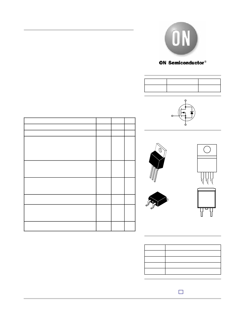
| 封装/外壳: | TO-263-3,D²Pak(2 引线+接片),TO-263AB |
| 供应商设备封装: | D2PAK |
| 包装: | 剪切带 (CT) |
| 其它名称: | NTB65N02RT4OSCT |
�� �
�
�NTB65N02R,� NTP65N02R�
�Power� MOSFET�
�65� A,� 24� V� N?Channel�
�TO?220,� D� 2� PAK�
�Features�
�?� Planar� HD3e� Process� for� Fast� Switching� Performance�
�?� Low� R� DSon� to� Minimize� Conduction� Loss�
�?� Low� C� iss� to� Minimize� Driver� Loss�
�?� Low� Gate� Charge�
�?� Pb?Free� Packages� are� Available*�
�MAXIMUM� RATINGS� (T� J� =� 25� °� C� Unless� otherwise� specified)�
�V� (BR)DSS�
�24� V�
�http://onsemi.com�
�R� DS(on)� TYP�
�8.4� m� W� @� 10� V�
�D�
�G�
�I� D� MAX�
�65� A�
�Parameter�
�Symbol�
�Value�
�Unit�
�Drain?to?Source� Voltage�
�Gate?to?Source� Voltage� ?� Continuous�
�Thermal� Resistance� ?� Junction?to?Case�
�Total� Power� Dissipation� @� T� C� =� 25� °� C�
�V� DSS�
�V� GS�
�R� q� JC�
�P� D�
�25�
�±� 20�
�2.0�
�62.5�
�V� dc�
�V� dc�
�°� C/W�
�W�
�S�
�MARKING�
�DIAGRAMS�
�Drain� Current� ?�
�Continuous� @� T� C� =� 25� °� C,� Chip�
�Continuous� @� T� C� =25� °� C,� Limited� by� Package�
�Single� Pulse� (t� p� =� 10� m� s)�
�I� D�
�I� D�
�I� DM�
�65�
�58�
�160�
�A�
�A�
�A�
�4�
�TO?220AB�
�Thermal� Resistance� ?�
�Junction?to?Ambient� (Note� 1)�
�Total� Power� Dissipation� @� T� A� =� 25� °� C�
�Drain� Current� ?� Continuous� @� T� A� =� 25� °� C�
�R� q� JA�
�P� D�
�I� D�
�67�
�1.86�
�10�
�°� C/W�
�W�
�A�
�CASE� 221A�
�STYLE� 5�
�P65N02RG�
�AYWW�
�Thermal� Resistance� ?�
�Junction?to?Ambient� (Note� 2)�
�Total� Power� Dissipation� @� T� A� =� 25� °� C�
�Drain� Current� ?� Continuous� @� T� A� =� 25� °� C�
�R� q� JA�
�P� D�
�I� D�
�120�
�1.04�
�7.6�
�°� C/W�
�W�
�A�
�1�
�2�
�3�
�Operating� and� Storage� Temperature� Range�
�Single� Pulse� Drain?to?Source� Avalanche�
�Energy� ?� Starting� T� J� =� 25� °� C�
�T� J� and�
�T� stg�
�E� AS�
�?55� to�
�150�
�60�
�°� C�
�mJ�
�2�
�1� 3�
�4�
�D� 2� PAK�
�CASE� 418AA�
�STYLE� 2�
�65N02RG�
�AYWW�
�(V� DD� =� 50� V� dc� ,� V� GS� =� 10� V� dc� ,� I� L� =� 11� A� pk� ,�
�L� =� 1� mH,� R� G� =� 25� W� )�
�65N02R� =� Specific� Device� Code�
�A� =� Assembly� Location�
�Maximum� Lead� Temperature� for� Soldering�
�Purposes,� 1/8� ″� from� Case� for� 10� Seconds�
�T� L�
�260�
�°� C�
�Y� =� Year�
�WW� =� Work� Week�
�G� =� Pb?Free� Package�
�Maximum� ratings� are� those� values� beyond� which� device� damage� can� occur.�
�Maximum� ratings� applied� to� the� device� are� individual� stress� limit� values� (not�
�normal� operating� conditions)� and� are� not� valid� simultaneously.� If� these� limits� are�
�exceeded,� device� functional� operation� is� not� implied,� damage� may� occur� and�
�PIN� ASSIGNMENT�
�reliability� may� be� affected.�
�1.� When� surface� mounted� to� an� FR4� board� using� 1� in.� pad� size,� (Cu� Area� 1.127� in� 2� ).�
�2.� When� surface� mounted� to� an� FR4� board� using� minimum� recommended� pad�
�size,� (Cu� Area� 0.412� in� 2� ).�
�PIN�
�1�
�2�
�FUNCTION�
�Gate�
�Drain�
�*For� additional� information� on� our� Pb?Free� strategy� and� soldering� details,� please�
�3�
�4�
�Source�
�Drain�
�ORDERING� INFORMATION�
�download� the� ON� Semiconductor� Soldering� and� Mounting� Techniques�
�Reference� Manual,� SOLDERRM/D.�
�See� detailed� ordering� and� shipping� information� in� the� package�
�dimensions� section� on� page� 5� of� this� data� sheet.�
�?� Semiconductor� Components� Industries,� LLC,� 2005�
�May,� 2005� ?� Rev.� 6�
�1�
�Publication� Order� Number:�
�NTB65N02R/D�
�相关PDF资料 |
PDF描述 |
|---|---|
| PVZ2R473C04R00 | TRIMMER 47K OHM 0.1W SMD |
| ASPI-0418S-100M-T3 | INDUCTOR POWER MINI 10UH 0418 |
| LB26WKW01-JF | SWITCH PUSHBUTTON DPDT 3A 125V |
| PVZ2R473C04B00 | TRIMMER 47K OHM 0.1W SMD |
| NTB125N02RT4 | MOSFET N-CH 24V 15.9A D2PAK |
相关代理商/技术参数 |
参数描述 |
|---|---|
| NTB65N02RT4G | 功能描述:MOSFET 24V 65A N-Channel RoHS:否 制造商:STMicroelectronics 晶体管极性:N-Channel 汲极/源极击穿电压:650 V 闸/源击穿电压:25 V 漏极连续电流:130 A 电阻汲极/源极 RDS(导通):0.014 Ohms 配置:Single 最大工作温度: 安装风格:Through Hole 封装 / 箱体:Max247 封装:Tube |
| NTB6N60 | 制造商:Rochester Electronics LLC 功能描述:- Bulk 制造商:ON Semiconductor 功能描述: |
| NTB6N60T4 | 制造商:Rochester Electronics LLC 功能描述:- Bulk |
| NTB707 | 制造商:未知厂家 制造商全称:未知厂家 功能描述:TRANSISTOR | BJT | PNP | 60V V(BR)CEO | 7A I(C) | TO-220AB |
| NTB708 | 制造商:未知厂家 制造商全称:未知厂家 功能描述:TRANSISTOR | BJT | PNP | 60V V(BR)CEO | 7A I(C) | TO-220AB |
发布紧急采购,3分钟左右您将得到回复。