- 您现在的位置:买卖IC网 > PDF目录189273 > NTE1549 (NTE Electronics, Inc.) Integrated Circuit Dot/Bar Display Driver PDF资料下载
参数资料
| 型号: | NTE1549 |
| 厂商: | NTE Electronics, Inc. |
| 英文描述: | Integrated Circuit Dot/Bar Display Driver |
| 中文描述: | 集成电路点/酒吧显示驱动程序 |
| 文件页数: | 2/4页 |
| 文件大小: | 29K |
| 代理商: | NTE1549 |
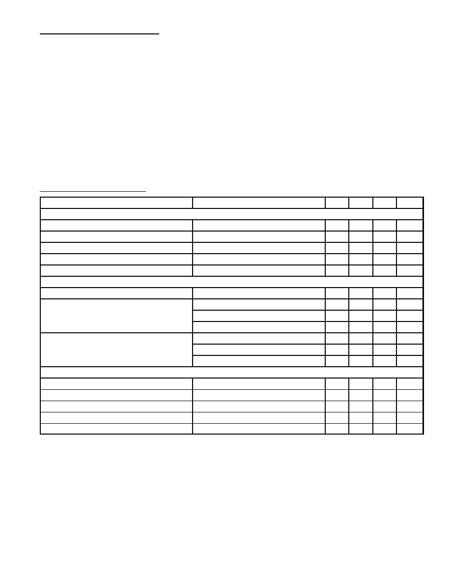
Absolute Maximum Ratings:
Power Dissipation (Note 1)
625mW
. . . . . . . . . . . . . . . . . . . . . . . . . . . . . . . . . . . . . . . . . . . . . . . . . . . . . . .
Supply Voltage
25V
. . . . . . . . . . . . . . . . . . . . . . . . . . . . . . . . . . . . . . . . . . . . . . . . . . . . . . . . . . . . . . . . . . . . .
Voltage on Output Drivers
25V
. . . . . . . . . . . . . . . . . . . . . . . . . . . . . . . . . . . . . . . . . . . . . . . . . . . . . . . . . . .
Input Signal Overvoltage (Note 2)
±35V
. . . . . . . . . . . . . . . . . . . . . . . . . . . . . . . . . . . . . . . . . . . . . . . . . . .
Divider Voltage
–100mV to V+
. . . . . . . . . . . . . . . . . . . . . . . . . . . . . . . . . . . . . . . . . . . . . . . . . . . . . . . . . . . .
Reference Load Current
10mA
. . . . . . . . . . . . . . . . . . . . . . . . . . . . . . . . . . . . . . . . . . . . . . . . . . . . . . . . . .
Storage Temperature Range
–55
° to +150°C
. . . . . . . . . . . . . . . . . . . . . . . . . . . . . . . . . . . . . . . . . . . . . . .
Lead Temperature (Soldering, 10 seconds)
+300
°C
. . . . . . . . . . . . . . . . . . . . . . . . . . . . . . . . . . . . . . . . .
Note 1. The maximum junction temperature of the NTE1549 is 100
°C. Devices must be derated for
operation at elevated temperatures. Junction to ambient thermal resistance is 120
°C/W.
Note 2. Pin 5 input current must be limited to
±3mA. The addition of a 39k resistor in series with Pin5
allows
±100V signals without damage.
Electrical Characteristics: (Note 3)
Parameter
Test Conditions
Min
Typ
Max
Unit
Comparators
Offset Voltage, Buffer and First Comparator
0V
≤ VRLO = VRHI ≤ 12V, ILED = 1mA
–
3
10
mV
Offset Voltage, Buffer and Any Other Comparator
0V
≤ VRLO = VRHI ≤ 12V, ILED = 1mA
–
3
15
mV
Gain (
ILED/VIN)
I(REF) = 2mA, ILED = 10mA
3
8
–
mA/mV
Input Bias Current (At Pin5)
0V
≤ VIN ≤ (V+ =1.5V)
–
25
100
nA
Input Signal Overvoltage
No Change in Display
–35
–
+35
V
Voltage Divider
Divider Resistance
Total Pin6 to Pin4
8
12
17
k
Relative Accuracy (Input Change Between Any Two
–1dB
≤ VIN ≤ 3dB, Note 4
0.75
1.0
1.25
dB
Threshold Points)
–7dB
≤ VIN ≤ –1dB, Note 4
1.5
2.0
2.5
dB
–10dB
≤ VIN ≤ –7dB, Note 4
2.5
3.0
2.5
dB
Absolute Accuracy
VIN = 2, 1, 0, –1dB
–0.25
–
+0.25
dB
VIN = –3, –5dB
–0.5
–
+0.5
dB
VIN = –7, –10, –20dB
–1
–
+1
dB
Voltage Reference
Output Voltage
0.1mA
≤ IL(REF) ≤ 4mA, V+ = VLED = 5V
1.2
1.28
1.34
V
Line Regulation
3V
≤ V+ ≤ 18V
–
0.01
0.03
%/V
Load Regulation
0.1mA
≤ IL(REF) ≤ 4mA, V+ = VLED = 5V
–
0.4
2.0
%
Output Voltage Change with Temperature
0
° ≤ TA ≤ +70°C, IL(REF) = 1mA, V+ = VLED = 5V
–
1
–
%
Adjust Pin Current
–
75
120
mA
Note 3. Unless otherwise stated, all specifications apply with the following conditions:
3VDC ≤ V+ ≤ 20VDC; –0.015V ≤ VRLO ≤ 12VDC; TA = +25°C, IL(REF) = 0.2mA, Pin9 con-
nected to Pin3 bar mode.
3VDC
≤ VLED ≤ V+; VREF, VRHI, VRLO ≤ (V+ –1.5V); For higher power dissipations, pulse
testing is used.
–0.015V
≤ VRHI ≤ 12VDC; 0V ≤ VIN ≤ V+ –1.5V
Note 4. Accuracy is measured referred to +3dB = +3dB = +10.000VDC at Pin5, with +10.000VDC at
Pin6, and 0.000 VDC at Pin4. At lower full–scale voltages, buffer and comparator offset volt-
age may add significant error.
相关PDF资料 |
PDF描述 |
|---|---|
| NTE1556 | Integrated Circuit VIR Signal Processor for Color TV |
| NTE1557 | CABLE TIE 40LB 11" GRAY NYLON 2-PC |
| NTE1559 | Integrated Circuit FM IF Amp, Demod |
| NTE1560 | Integrated Circuit Phase Lock Loop (PLL) FM Stereo Multiplex Demodulator |
| NTE1561 | Integrated Circuit 5 LED VU Level Meter |
相关代理商/技术参数 |
参数描述 |
|---|---|
| NTE155 | 制造商:NTE Electronics 功能描述:TO-66 NPN AUD PWR 制造商:NTE Electronics 功能描述:Trans GP BJT NPN 32V 1A 2-Pin(2+Tab) TO-66 |
| NTE1550 | 制造商:NTE Electronics 功能描述:IC-TV SIGNAL PROCESSOR 制造商:NTE Electronics 功能描述:DIP-16+2 SYN SIG PRO 制造商:NTE Electronics 功能描述:IC, VIDEO SYNC; Output Synch Type:Horizontal, Vertical; Supply Voltage Max:16V; TV / Video Case Style:DIP; No. of Pins:18; Operating Temperature Min:-20C; Operating Temperature Max:75C; Operating Temperature Range:-20C to +75C 制造商:NTE Electronics 功能描述:Analog Signal Processor 18-Pin |
| NTE1551 | 制造商:NTE Electronics 功能描述:IF Amplifier 16-Pin(16+Tab) DIP |
| NTE1553 | 制造商:未知厂家 制造商全称:未知厂家 功能描述:Analog IC |
| NTE1554 | 制造商:NTE Electronics 功能描述:IC MOTOR DRVR; Motor Type:-; Driver Case Style:-; Supply Voltage Range:- |
发布紧急采购,3分钟左右您将得到回复。