- 您现在的位置:买卖IC网 > PDF目录363709 > NTE943 (NTE Electronics, Inc.) Integrated Circuit Low Power, Low Offset, Dual Voltage Comparator PDF资料下载
参数资料
| 型号: | NTE943 |
| 厂商: | NTE Electronics, Inc. |
| 英文描述: | Integrated Circuit Low Power, Low Offset, Dual Voltage Comparator |
| 中文描述: | 集成电路低功耗,低失调,双电压比较器 |
| 文件页数: | 2/5页 |
| 文件大小: | 35K |
| 代理商: | NTE943 |
Absolute Maximum Ratings:
Supply Voltage, V+
Differential Input Voltage (Note 1)
Input Voltage
. . . . . . . . . . . . . . . . . . . . . . . . . . . . . . . . . . . . . . . . . . . . . . . . . . . . . . . . . . . . .
Power Dissipation (Note 2)
NTE943
. . . . . . . . . . . . . . . . . . . . . . . . . . . . . . . . . . . . . . . . . . . . . . . . . . . . . . . . . . . . . . . . .
NTE943M
. . . . . . . . . . . . . . . . . . . . . . . . . . . . . . . . . . . . . . . . . . . . . . . . . . . . . . . . . . . . . . .
NTE943SM
. . . . . . . . . . . . . . . . . . . . . . . . . . . . . . . . . . . . . . . . . . . . . . . . . . . . . . . . . . . . . .
Output Short Circuit to GND (Note 3)
. . . . . . . . . . . . . . . . . . . . . . . . . . . . . . . . . . . . . . . . . .
Input Current (V
IN
<
–
0.3V), Note 4)
. . . . . . . . . . . . . . . . . . . . . . . . . . . . . . . . . . . . . . . . . . . . . . . .
Operating Temperature Range
. . . . . . . . . . . . . . . . . . . . . . . . . . . . . . . . . . . . . . . . . . . . . . .
Storage Temperature Range
. . . . . . . . . . . . . . . . . . . . . . . . . . . . . . . . . . . . . . . . . . . . . .
Lead Temperature (During Soldering, 10 sec)
36V or
±
18V
. . . . . . . . . . . . . . . . . . . . . . . . . . . . . . . . . . . . . . . . . . . . . . . . . . . . . . . . .
. . . . . . . . . . . . . . . . . . . . . . . . . . . . . . . . . . . . . . . . . . . . . . . . . . . .
36V
–
0.3V to +36V
660mW
780mW
510mW
Continuous
50mA
0
°
to +70
°
C
–
65
°
to +150
°
C
+260
°
C
. . . . . . . . . . . . . . . . . . . . . . . . . . . . . . . . . . . . . .
Note 1. Positive excursions of input voltage may exceed the power supply level. As long as the other
voltage remains within the common
–
mode range, the comparator will provide a proper out-
put state. The low input voltage state must not be less than
–
0.3V (or 0.3V below the the
magnitude of the negative power supply, if used).
Note 2. For operating at elevated temperature, these devices must be derated based on a 125
°
C
maximum junction temperature and a thermal resistance of 127
°
C/W which applies for the
device soldered in a printed circuit board, operating in a still air ambient. The low bias dis-
sipation and the
“
ON
–
OFF
”
haracteristic of the output keeps the chip dissipation very small
(P
D
≤
100mW), provided the output transistors are allowed to saturate.
Note 3. Short circuits from the output to V+ can cause excessive heating and eventual destruction.
When considering short circuits to GND, the maximum output current is approximately 20mA
independent of the magnitude of V+.
Note 4. This input current will only exist when the voltage at any of th input leads is driven negative.
It is due to the collector
–
base junction of the input PNP transistors becoming forward biased
and thereby acting as input diode clamps. In addition to this diode action, there is also lateral
NPN parasitic transistor action on the IC chip. This transistor action can cause the output
voltages of the comparators to go to the V+ voltage level (or to GND for a large overdrive)
for the time duration that an input is driven negative. This is not destructive and normal out-
put states will re
–
establish when the input voltage, which was negative, again returns to a
value greater than
–
0.3V.
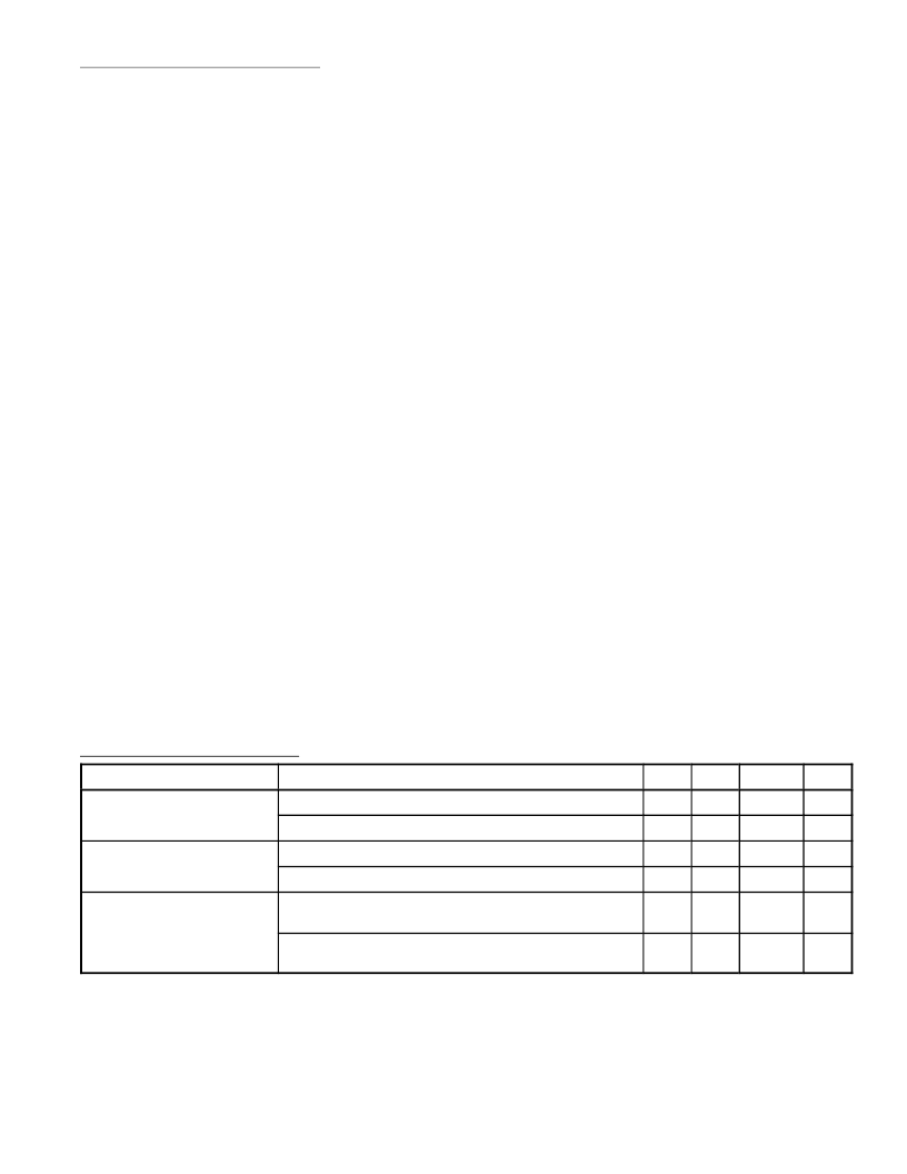
Electrical Characteristics:
(0
°
≤
T
A
≤
+70
°
C, V+ = 5V unless otherwise specified)
Parameter
Test Conditions
Min
Typ
Max
±
9.0
±
5.0
±
150
±
50
250
Unit
Input Offset Voltage
Note 5
T
A
= +25
°
C, Note 5
I
IN
(+)
–
I
IN
(
–
) V
CM
= 0V
I
IN
(+)
–
I
IN
(
–
) V
CM
= 0V, T
A
= +25
°
C
I
IN
(+) or I
IN
(
–
) with Output in Linear Range, V
CM
= 0V,
Note 6
–
–
mV
–
±
1.0
–
±
5.0
–
mV
Input Offset Current
–
nA
–
nA
Input Bias Current
–
nA
I
IN
(+) or I
IN
(
–
) with Output in Linear Range, V
CM
= 0V,
T
A
= +25
°
C, Note 6
–
25
250
nA
Note 5. At output switch point, V
O
common
–
mode range (0V to V+
–
1.5V), at 25
°
C.
1.4V, R
S
= 0
, with V+ from 5V to 30V and over he full input
Note 6. The direction of the input current is out of the IC due to the PNP input stage. This current
is essentially constant, independent of the state of the output so no loading change exists
on the reference or input lines.
相关PDF资料 |
PDF描述 |
|---|---|
| NTE943M | Integrated Circuit Low Power, Low Offset, Dual Voltage Comparator |
| NTE943SM | Integrated Circuit Low Power, Low Offset, Dual Voltage Comparator |
| NTE944 | Integrated Circuit Programmable Operational Amplifier |
| NTE944M | Integrated Circuit Programmable Operational Amplifier |
| NTE947 | Integrated Circuit Dual Operational Amplifier |
相关代理商/技术参数 |
参数描述 |
|---|---|
| NTE943M | 制造商:NTE Electronics 功能描述:IC PRECISION COMP DUAL 1.3 uS DIP-8 制造商:NTE Electronics 功能描述:IC, PRECISION COMP, DUAL, 1.3 uS, DIP-8 制造商:NTE Electronics 功能描述:IC-DUAL COMPARATOR-8P-DIP 制造商:NTE Electronics 功能描述:DIP-8 LOW PWR V-COMP 制造商:NTE Electronics 功能描述:IC, PRECISION COMP, DUAL, 1.3 uS, DIP-8; Comparator Type:Precision; No. of Comparators:2; Response Time:1.3s; Supply Voltage Range: 1V to 18V; Amplifier Case Style:DIP; No. of Pins:8; IC Output Type:CMOS, MOS, TTL, DTL, ECL ;RoHS Compliant: Yes 制造商:NTE Electronics 功能描述:Comparator Dual ±18V/36V 8-Pin Mini-DIP |
| NTE943SM | 制造商:NTE Electronics 功能描述:IC-DUAL COMPARATOR 制造商:NTE Electronics 功能描述:Comparator Dual ±18V/36V 8-Pin SOIC |
| NTE944 | 制造商:NTE Electronics 功能描述:IC-PROG OP AMP 制造商:NTE Electronics 功能描述:OP Amp Single GP ±18V 8-Pin Metal Can |
| NTE944M | 制造商:NTE Electronics 功能描述:Bulk 制造商:NTE Electronics 功能描述:IC-PROG OP AMP 制造商:NTE Electronics 功能描述:DIP-8 PROG OP AMP 制造商:NTE Electronics 功能描述:OP Amp Single GP ±18V 8-Pin Mini-PDIP |
| NTE945 | 制造商:NTE Electronics 功能描述:IC-HI IMPEDANCE OP-AMP |
发布紧急采购,3分钟左右您将得到回复。