- 您现在的位置:买卖IC网 > PDF目录18326 > NTJD5121NT1G (ON Semiconductor)MOSFET N-CH DUAL 60V SOT-363 PDF资料下载
参数资料
| 型号: | NTJD5121NT1G |
| 厂商: | ON Semiconductor |
| 文件页数: | 1/5页 |
| 文件大小: | 0K |
| 描述: | MOSFET N-CH DUAL 60V SOT-363 |
| 标准包装: | 1 |
| FET 型: | 2 个 N 沟道(双) |
| FET 特点: | 逻辑电平门 |
| 漏极至源极电压(Vdss): | 60V |
| 电流 - 连续漏极(Id) @ 25° C: | 295mA |
| 开态Rds(最大)@ Id, Vgs @ 25° C: | 1.6 欧姆 @ 500mA,10V |
| Id 时的 Vgs(th)(最大): | 2.5V @ 250µA |
| 闸电荷(Qg) @ Vgs: | 0.9nC @ 4.5V |
| 输入电容 (Ciss) @ Vds: | 26pF @ 20V |
| 功率 - 最大: | 250mW |
| 安装类型: | 表面贴装 |
| 封装/外壳: | 6-TSSOP,SC-88,SOT-363 |
| 供应商设备封装: | SC-88 |
| 包装: | 标准包装 |
| 其它名称: | NTJD5121NT1GOSDKR |
�� �
�
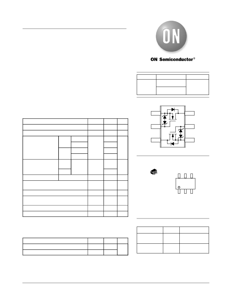
�NTJD5121N�
�Power� MOSFET�
�60� V,� 295� mA,� Dual� N� ?� Channel� with� ESD�
�Protection,� SC� ?� 88�
�Features�
�?� Low� R� DS(on)�
�?� Low� Gate� Threshold�
�?� Low� Input� Capacitance�
�?� ESD� Protected� Gate�
�?� This� is� a� Pb� ?� Free� Device�
�Applications�
�?� Low� Side� Load� Switch�
�?� DC� ?� DC� Converters� (Buck� and� Boost� Circuits)�
�V� (BR)DSS�
�60� V�
�http://onsemi.com�
�R� DS(on)� MAX�
�1.6� W� @� 10� V�
�2.5� W� @� 4.5� V�
�SC� ?� 88� (SOT� ?� 363)�
�I� D� Max�
�295� mA�
�MAXIMUM� RATINGS� (T� J� =� 25� °� C� unless� otherwise� stated)�
�Symbol�
�Parameter�
�Value�
�Unit�
�S� 1�
�1�
�6�
�D� 1�
�Drain� ?� to� ?� Source� Voltage�
�V� DSS�
�60�
�V�
�G� 1�
�2�
�5�
�G� 2�
�Gate� ?� to� ?� Source� Voltage�
�V� GS�
�±� 20�
�V�
�Continuous� Drain�
�Current� (Note� 1)�
�Steady�
�State�
�T� A� =� 25� °� C�
�T� A� =� 85� °� C�
�I� D�
�295�
�212�
�mA�
�D� 2�
�3�
�4�
�S� 2�
�t� ≤� 5s�
�T� A� =� 25� °� C�
�T� A� =� 85� °� C�
�304�
�219�
�Top� View�
�Power� Dissipation�
�(Note� 1)�
�Steady�
�State�
�T� A� =� 25� °� C�
�P� D�
�250�
�mW�
�MARKING� DIAGRAM� &�
�PIN� ASSIGNMENT�
�Pulsed� Drain� Current�
�t� ≤� 5s�
�t� p� =� 10� m� s�
�I� DM�
�266�
�900�
�mA�
�1�
�6�
�D1� G2� S2�
�Operating� Junction� and� Storage� Temperature�
�Source� Current� (Body� Diode)�
�T� J� ,� T� STG�
�I� S�
�?� 55� to�
�150�
�210�
�°� C�
�mA�
�SC� ?� 88/SOT� ?� 363�
�CASE� 419B�
�STYLE� 26�
�1�
�TF� M� G�
�G�
�Lead� Temperature� for� Soldering� Purposes�
�(1/8”� from� case� for� 10� s)�
�Gate� ?� Source� ESD� Rating� (HBM)�
�T� L�
�ESD� HBM�
�260�
�2000�
�°� C�
�V�
�TF�
�M�
�G�
�S1� G1� D2�
�=� Device� Code�
�=� Date� Code�
�=� Pb� ?� Free� Package�
�Gate� ?� Source� ESD� Rating� (MM)�
�ESD� MM�
�200�
�V�
�(Note:� Microdot� may� be� in� either� location)�
�Stresses� exceeding� Maximum� Ratings� may� damage� the� device.� Maximum�
�Ratings� are� stress� ratings� only.� Functional� operation� above� the� Recommended�
�Operating� Conditions� is� not� implied.� Extended� exposure� to� stresses� above� the�
�Recommended� Operating� Conditions� may� affect� device� reliability.�
�ORDERING� INFORMATION�
�Device� Package� Shipping� ?�
�THERMAL� RESISTANCE� RATINGS�
�NTJD5121NT1G�
�SC� ?� 88�
�3000� /� Tape� &� Reel�
�Parameter�
�Symbol�
�Value�
�Unit�
�(Pb� ?� Free)�
�Junction� ?� to� ?� Ambient� –� Steady� State� R� q� JA�
�Junction� ?� to� ?� Ambient� –� t� ≤� 5� s� R� q� JA�
�1.� Surface� mounted� on� FR4� board� using� 1� in� sq� pad� size�
�(Cu� area� =� 1.127� in� sq� [2� oz]� including� traces).�
�?� Semiconductor� Components� Industries,� LLC,� 2013�
�October,� 2013� ?� Rev.� 6�
�500�
�470�
�1�
�°� C/W�
�NTJD5121NT2G� SC� ?� 88� 3000� /� Tape� &� Reel�
�(Pb� ?� Free)�
�?For� information� on� tape� and� reel� specifications,�
�including� part� orientation� and� tape� sizes,� please�
�refer� to� our� Tape� and� Reel� Packaging� Specification�
�Brochure,� BRD8011/D.�
�Publication� Order� Number:�
�NTJD5121N/D�
�相关PDF资料 |
PDF描述 |
|---|---|
| B32652A1682K | FILM CAP 6.8NF 10% 1600V MKP |
| B32652A1612J | FILM CAP 6.1NF 5% 1600V |
| B32621A6472K | FILM CAP 0.0047UF 10% 630V |
| B32621A6103K | FILM CAP 0.0100UF 10% 630V |
| B32620A6681J | FILM CAP 0.00068UF 5% 630V |
相关代理商/技术参数 |
参数描述 |
|---|---|
| NTJD5121NT2G | 功能描述:MOSFET NFET SC88D 60V 295mA RoHS:否 制造商:STMicroelectronics 晶体管极性:N-Channel 汲极/源极击穿电压:650 V 闸/源击穿电压:25 V 漏极连续电流:130 A 电阻汲极/源极 RDS(导通):0.014 Ohms 配置:Single 最大工作温度: 安装风格:Through Hole 封装 / 箱体:Max247 封装:Tube |
| NTJS3151P | 制造商:ONSEMI 制造商全称:ON Semiconductor 功能描述:Trench Power MOSFET 12 V, 3.3 A, Single P−Channel, ESD Protected SC−88 |
| NTJS3151PT1 | 功能描述:MOSFET 12V 3.3A P-Channel RoHS:否 制造商:STMicroelectronics 晶体管极性:N-Channel 汲极/源极击穿电压:650 V 闸/源击穿电压:25 V 漏极连续电流:130 A 电阻汲极/源极 RDS(导通):0.014 Ohms 配置:Single 最大工作温度: 安装风格:Through Hole 封装 / 箱体:Max247 封装:Tube |
| NTJS3151PT1G | 功能描述:MOSFET 12V 3.3A P-Channel RoHS:否 制造商:STMicroelectronics 晶体管极性:N-Channel 汲极/源极击穿电压:650 V 闸/源击穿电压:25 V 漏极连续电流:130 A 电阻汲极/源极 RDS(导通):0.014 Ohms 配置:Single 最大工作温度: 安装风格:Through Hole 封装 / 箱体:Max247 封装:Tube |
| NTJS3151PT2 | 功能描述:MOSFET 12V 3.3A P-Channel RoHS:否 制造商:STMicroelectronics 晶体管极性:N-Channel 汲极/源极击穿电压:650 V 闸/源击穿电压:25 V 漏极连续电流:130 A 电阻汲极/源极 RDS(导通):0.014 Ohms 配置:Single 最大工作温度: 安装风格:Through Hole 封装 / 箱体:Max247 封装:Tube |
发布紧急采购,3分钟左右您将得到回复。